DM385, DM388
www.ti.com
SPRS821D –MARCH 2013–REVISED DECEMBER 2013
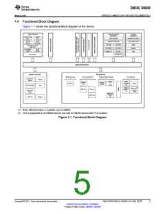
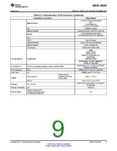
1.4 Functional Block Diagram
Figure 1-1 shows the functional block diagram of the device.
Video Processing
Subsystem
Imaging
Subsystem
ARM Subsystem
CortexTM -A8
CPU
NEON
FPU
Video Capture
Parallel Cam Input
CSI2 Serial Input
IPIPE
32 KB
I-Cache
32 KB
D-Cache
Display Processing
HD OSD
SD OSD
256 KB L2 Cache
with ECC
HD VENC
HDMI Xmt
SD VENC
Resizer
Boot ROM
48 KB
RAM
64 KB
SD DAC
H3A
ICE Crusher
HD DAC (3)
System Interconnect
Peripherals
System Control
Real-Time
Clock
Program/Data Storage
Connectivity
Miscellaneous
Serial Interfaces
PRCM
EMAC
(R)(G)MII
(2)
GPMC
McASP
(2)
DDR2/3
+
GPIO (4)
MDIO
32-bit
ELM
GP Timer (8)
JTAG
(2)
USB 2.0
Ctrl/PHY
(2)
2
PCIe 2.0
(One x1
Port)
SPI (4)
I
C (4)
Watchdog
Timer
MMC/SD/
SDIO
(3)
UART (3)
Spinlock
Mailbox
(1) Noise Filtering Engine is available only on DM388.
(2) PCIe is supported on all DM385 devices and also on DM388 devices with PCIe enabled.
Figure 1-1. Functional Block Diagram
Copyright © 2013, Texas Instruments Incorporated
High-Performance System-on-Chip (SoC)
5
Submit Documentation Feedback
Product Folder Links: DM385 DM388

 TI [ TEXAS INSTRUMENTS ]