DLPA2000
www.ti.com.cn
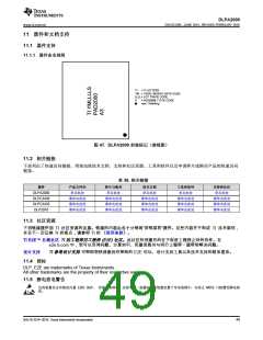
ZHCSCO5B –JUNE 2014–REVISED FEBRUARY 2018
10 Layout
10.1 Layout Guidelines
As for all chips with switching power supplies, the layout is an important step in the design, especially in the case
of high peak currents and high switching frequencies. If the layout is not carefully done, the regulators could
show stability problems as well as EMI problems. Therefore, use wide and short traces for the main current paths
and for the power ground tracks. Input capacitors, output capacitors, and inductors should be placed as close as
possible to the IC.
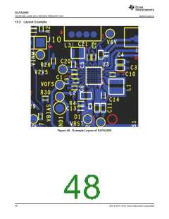
Figure 46 shows an example layout that has critical parts placed as close as possible to the pins they are
connected to. Here are recommendations for the following components:
R1
is RLIM and is connected via a wide trace and as short as possible to the DLPA2000 and the ground.
is the big inductor for the VLED that is connected via two wide traces to the pins.
L1
C3/C4
are the decoupling capacitors for the VLED and they are as close as possible placed to the part and
directly connected to ground.
L3/C20 are components used for the VCORE BUCK. L3 is placed close to the pin and connected with a wide
trace to the part. C20 is placed directly beside the inductor and connected to the PGND pin.
L2
This inductor is part of the DMD reset regulators and is also placed as close as possible to the
DLPA2000 using wide PCB traces.
版权 © 2014–2018, Texas Instruments Incorporated
47

 TI [ TEXAS INSTRUMENTS ]