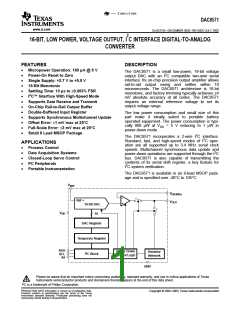
DAC8571
www.ti.com
SLAS373A–DECEMBER 2002–REVISED JULY 2003
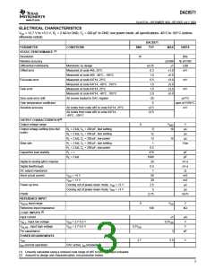
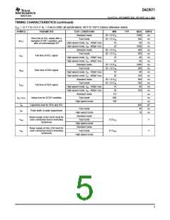
ELECTRICAL CHARACTERISTICS
VDD = +2.7 V to +5.5 V; RL = 2 kΩ to GND; CL = 200 pF to GND; low power mode; all specifications -40°C to 105°C (unless
otherwise noted)
DAC8571
PARAMETER
CONDITIONS
MIN
TYP
MAX
UNITS
(1)
STATIC PERFORMANCE
Resolution
16
Bits
% of FSR
LSB
Relative accuracy
Differential nonlinearity
Offset error
±0.098
±1
Monotonic by design
±0.25
0.3
Measured at code 485, 25°C
±1.0
±5.0
±3.0
±5.0
±3.0
±5.0
mV
Measured at code 485, -40°C...105°C
Measured at code 64714, 25°C
Measured at code 64714, -40°C...105°C
Measured at code 64714, 25°C
Measured at code 64714, -40°C...105°C
All zeroes loaded to DAC register
1.0
Full-scale error
Gain error
0.5
mV
mV
1.0
1.0
2.0
Zero code error drift
-20
-5
µV/°C
ppm of FSR/°C
mV
Gain temperature coefficient
Absolute accuracy
All codes from code 485 to code 64714, 25°C
±2.5
±3.5
All codes from code 485 to code 64714,
-40°C...105°C
OUTPUT CHARACTERISTICS(2)
Output voltage range
0
VREF
10
V
µs
Output voltage settling time (full
scale)
RL = 2 kΩ; CL < 200 pF, fast settling
RL = 2 kΩ; CL = 500 pF, fast settling
RL = 2 kΩ; CL < 200 pF, low power
RL = 2 kΩ; CL < 200 pF, fast settling
RL = 2 kΩ; CL < 200 pF, low power
RL = ∞
8
12
µs
13
15
µs
Slew rate
1
V/µs
0.5
470
1000
20
Capacitive load stability
pF
pF
RL = 2 kΩ
Digital-to-analog glitch impulse
Digital feedthrough
nV-s
nV-s
Ω
0.5
1
DC output impedance
Short circuit current
VDD = +5 V
50
mA
mA
µs
VDD = +3 V
20
Power-up time
Coming out of power-down mode, VDD = +5 V
Coming out of power-down mode, VDD = +3 V
2.5
5
µs
PSRR
0.75
mV/V
REFERENCE INPUT
VREFH input range
Reference input impedance
0
VDD
V
140
kΩ
(2)
LOGIC INPUTS
Input current
±1
µA
V
VIN_L, Input low voltage
VIN_H0 , Input high voltage
Pin capacitance
VDD = 2.7-5.5 V
VDD = 2.7-5.5 V
0.3VDD
0.7VDD
2.7
V
3
pF
POWER REQUIREMENTS
VDD
5.5
V
IDD (normal operation)
DAC active, Iref included
(1) Linearity calculated using a reduced code range of 485 to 64714. Output unloaded.
(2) Assured by design and characterization, not production tested.
3

 TI [ TEXAS INSTRUMENTS ]