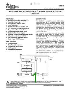
DAC8571
www.ti.com
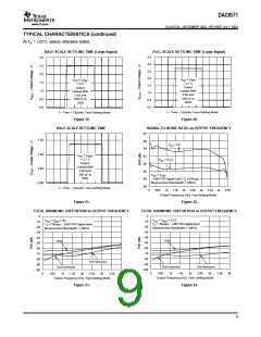
SLAS373A–DECEMBER 2002–REVISED JULY 2003
These devices have limited built-in ESD protection. The leads should be shorted together or the device
placed in conductive foam during storage or handling to prevent electrostatic damage to the MOS gates.
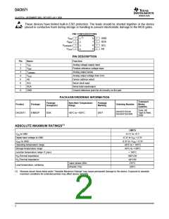
PIN CONFIGURATIONS
V
GND
SDA
SCL
A0
8
7
6
5
1
2
3
4
DD
V
REF
V
(SENSE)
V
OUT
PIN DESCRIPTION
Pin
1
Name
VDD
Function
Analog voltage supply input
2
VREF
V(SENSE)
VOUT
A0
Positive reference voltage input
Analog output sense
3
4
Analog output voltage from DAC
Device address select
5
6
SCL
Serial clock input
7
SDA
GND
Serial data input/output
8
Ground reference point for all circuitry on the part
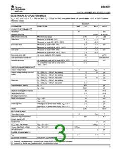
PACKAGE/ORDERING INFORMATION
Transport
Media,
Quantity
Package
Designator
Specified Temperature
Range
Package
Marking
Product
Package
Ordering Number
Tube, 80
Tape & Reel,
2500
DAC8571IDGK
DAC8571IDGKR
DAC8571
8-MSOP
DGK
-40°C to +105°C
D871
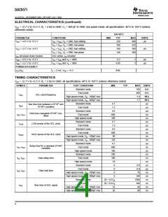
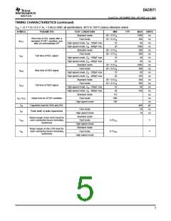
ABSOLUTE MAXIMUM RATINGS(1)
UNITS
VDD to GND
-0.3 V to +6 V
Digital input voltage to GND
VOUT to GND
-0.3V to VDD + 0.3V
-0.3V to +VDD + 0.3V
-40°C to + 105°C
-65°C to +150°C
+ 150°C
Operating temperature range
Storage temperature range
Junction temperature range (TJmax)
ΘJAThermal impedance
ΘJCThermal impedance
260°C/W
44°C/W
Vapor phase (60s)
Infrared (15s)
215°C
Lead temperature, soldering
220°C
(1) Stresses above those listed under “Absolute Maximum Ratings” may cause permanent damage to the device. Exposure to absolute
maximum conditions for extended periods may affect device reliability.
2

 TI [ TEXAS INSTRUMENTS ]