CC2640R2L
ZHCSRK4A –APRIL 2020 –REVISED SEPTEMBER 2020
www.ti.com.cn
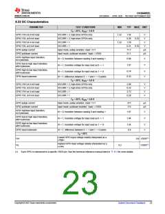
8.21 Synchronous Serial Interface (SSI)
Tc = 25°C, VDDS = 3.0 V, unless otherwise noted.
PARAMETER
TEST CONDITIONS
Device operating as slave
Device operating as slave
MIN
TYP
MAX
UNIT
system
clocks
S1(1) tclk_per (SSIClk period)
12
65024
S2(1) tclk_high (SSIClk high time)
S3(1) tclk_low (SSIClk low time)
0.5
0.5
tclk_per
tclk_per
Device operating as slave
One-way communication to slave, device
operating as master
system
clocks
S1 (TX only)(1) tclk_per (SSIClk period)
S1 (TX and RX)(1) tclk_per (SSIClk period)
4
8
65024
65024
Normal duplex operation, device operating
as master
system
clocks
S2(1) tclk_high (SSIClk high time)
S3(1) tclk_low (SSIClk low time)
Device operating as master
Device operating as master
0.5
0.5
tclk_per
tclk_per
(1) Refer to SSI timing diagrams 图8-1, 图8-2, and 图8-3.
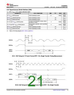
S1
S2
SSIClk
S3
SSIFss
SSITx
MSB
LSB
SSIRx
4 to 16 bits
图8-1. SSI Timing for TI Frame Format (FRF = 01), Single Transfer Timing Measurement
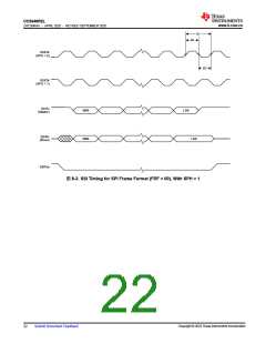
S2
S1
SSIClk
SSIFss
SSITx
SSIRx
S3
MSB
LSB
8-bit control
0
MSB
LSB
4 to 16 bits output data
图8-2. SSI Timing for MICROWIRE Frame Format (FRF = 10), Single Transfer
Copyright © 2023 Texas Instruments Incorporated
Submit Document Feedback
21

 TI [ TEXAS INSTRUMENTS ]