CC2640R2L
ZHCSRK4A –APRIL 2020 –REVISED SEPTEMBER 2020
www.ti.com.cn
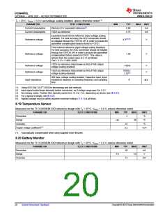
8.23 Thermal Resistance Characteristics
NAME
RθJA
DESCRIPTION
Junction-to-ambient thermal resistance
RHB (°C/W)(1) (2)
RGZ (°C/W)(1) (2)
32.8
24.0
6.8
29.6
15.7
6.2
Junction-to-case (top) thermal resistance
Junction-to-board thermal resistance
RθJC(top)
RθJB
PsiJT
Junction-to-top characterization parameter
Junction-to-board characterization parameter
Junction-to-case (bottom) thermal resistance
0.3
0.3
PsiJB
6.8
6.2
1.9
1.9
RθJC(bot)
(1) °C/W = degrees Celsius per watt.
(2) These values are based on a JEDEC-defined 2S2P system (with the exception of the Theta JC [RθJC] value, which is based on a
JEDEC-defined 1S0P system) and will change based on environment as well as application. For more information, see these EIA/
JEDEC standards:
•
•
•
•
JESD51-2, Integrated Circuits Thermal Test Method Environmental Conditions - Natural Convection (Still Air).
JESD51-3, Low Effective Thermal Conductivity Test Board for Leaded Surface Mount Packages.
JESD51-7, High Effective Thermal Conductivity Test Board for Leaded Surface Mount Packages.
JESD51-9, Test Boards for Area Array Surface Mount Package Thermal Measurements.
Power dissipation of 2 W and an ambient temperature of 70°C is assumed.
8.24 Timing Requirements
MIN
0
NOM
MAX UNIT
100 mV/µs
20 mV/µs
Rising supply-voltage slew rate
Falling supply-voltage slew rate
0
Falling supply-voltage slew rate, with low-power flash settings(1)
3
mV/µs
No limitation for negative
temperature gradient, or
outside standby mode
Positive temperature gradient in standby(2)
5
°C/s
CONTROL INPUT AC CHARACTERISTICS(3)
RESET_N low duration
1
µs
(1) For smaller coin cell batteries, with high worst-case end-of-life equivalent source resistance, a 22-µF VDDS input capacitor (see 图
10-1) must be used to ensure compliance with this slew rate.
(2) Applications using RCOSC_LF as sleep timer must also consider the drift in frequency caused by a change in temperature (see 节
8.17).
(3) TA = –40°C to +85°C, VDDS = 1.7 V to 3.8 V, unless otherwise noted.
8.25 Switching Characteristics
Measured on the TI CC2650EM-5XD reference design with Tc = 25°C, VDDS = 3.0 V, unless otherwise noted.
PARAMETER
TEST CONDITIONS
MIN
TYP
MAX
UNIT
WAKEUP AND TIMING
14
151
µs
µs
µs
Idle →Active
Standby →Active
Shutdown →Active
1015
Copyright © 2023 Texas Instruments Incorporated
24
Submit Document Feedback

 TI [ TEXAS INSTRUMENTS ]