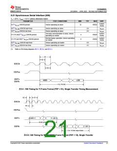
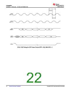
CC2640R2L
ZHCSRK4A –APRIL 2020 –REVISED SEPTEMBER 2020
www.ti.com.cn
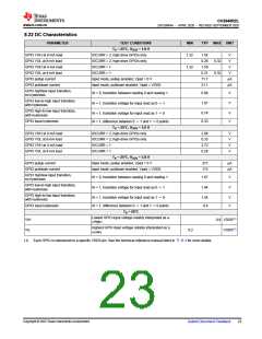
Tc = 25°C, VDDS = 3.0 V and voltage scaling enabled, unless otherwise noted.(1)
PARAMETER
TEST CONDITIONS
Internal 4.3-V equivalent reference(2)
VDDS as reference
MIN
TYP
0.66
0.75
MAX UNIT
Current consumption
Current consumption
mA
mA
Equivalent fixed internal reference (input voltage scaling
enabled). For best accuracy, the ADC conversion should
be initiated through the TIRTOS API in order to include the
gain/offset compensation factors stored in FCFG1.
Reference voltage
4.3(2) (5)
V
Fixed internal reference (input voltage scaling disabled).
For best accuracy, the ADC conversion should be initiated
through the TIRTOS API in order to include the gain/offset
compensation factors stored in FCFG1. This value is
derived from the scaled value (4.3 V) as follows:
Vref = 4.3 V × 1408 / 4095
Reference voltage
1.48
V
VDDS as reference (Also known as RELATIVE) (input
voltage scaling enabled)
Reference voltage
Reference voltage
VDDS
V
V
VDDS as reference (Also known as RELATIVE) (input
voltage scaling disabled)
VDDS /
2.82(5)
200 ksps, voltage scaling enabled. Capacitive input, Input
impedance depends on sampling frequency and sampling
time
Input impedance
>1
MΩ
(1) Using IEEE Std 1241™-2010 for terminology and test methods.
(2) Input signal scaled down internally before conversion, as if voltage range was 0 to 4.3 V.
(3) No missing codes. Positive DNL typically varies from +0.3 to +3.5, depending on device (see 图8-21).
(4) For a typical example, see 图8-22.
(5) Applied voltage must be within absolute maximum ratings (节8.1) at all times.
8.19 Temperature Sensor
Measured on the TI CC2650EM-5XD reference design with Tc = 25°C, VDDS = 3.0 V, unless otherwise noted.
PARAMETER
TEST CONDITIONS
MIN
TYP
MAX
UNIT
°C
Resolution
Range
4
85
°C
–40
Accuracy
±5
°C
Supply voltage coefficient(1)
3.2
°C/V
(1) Automatically compensated when using supplied driver libraries.
8.20 Battery Monitor
Measured on the TI CC2650EM-5XD reference design with Tc = 25°C, VDDS = 3.0 V, unless otherwise noted.
PARAMETER
TEST CONDITIONS
MIN
TYP
MAX
UNIT
mV
V
Resolution
Range
50
1.8
3.8
Accuracy
13
mV
Copyright © 2023 Texas Instruments Incorporated
20
Submit Document Feedback

 TI [ TEXAS INSTRUMENTS ]