CC1110Fx / CC1111Fx
3
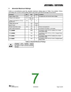
Absolute Maximum Ratings
Under no circumstances must the absolute maximum ratings given in Table 2 be violated. Stress
exceeding one or more of the limiting values may cause permanent damage to the device.
Parameter
Min
Max
Units Condition
Supply voltage (VDD)
Voltage on any digital pin
−0.3
3.9
V
V
All supply pins must have the same voltage
−0.3 VDD + 0.3,
max 3.9
Voltage on the pins RF_P, RF_N
and DCOUPL
−0.3
−50
2.0
V
Voltage ramp-up rate
Input RF level
120
10
kV/µs
dBm
C
Storage temperature range
Solder reflow temperature
ESD CC1110Fx
150
260
1000
Device not programmed
According to IPC/JEDEC J-STD-020D
C
V
According to JEDEC STD 22, method A114, Human
Body Model (HBM)
750
750
750
V
V
V
According to JEDEC STD 22, C101C, Charged Device
Model (CDM)
ESD CC1110Fx
ESD CC1111x
ESD CC1111x
According to JEDEC STD 22, method A114, Human
Body Model (HBM)
According to JEDEC STD 22, C101C, Charged Device
Model (CDM)
Table 2: Absolute Maximum Ratings
Caution!
ESD
sensitive
device.
Precaution should be used when handling
the device in order to prevent permanent
damage.
SWRS033H
Page 7 of 246

 TI [ TEXAS INSTRUMENTS ]