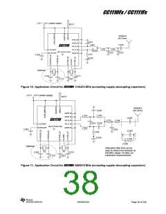
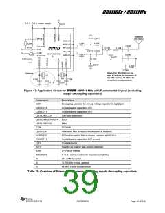
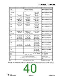
CC1110Fx / CC1111Fx
9.7 PCB Layout Recommendations
The top layer should be used for signal routing,
and the open areas should be filled with
metallization connected to ground using
several vias.
Each decoupling capacitor should be placed
as close as possible to the supply pin it is
supposed to decouple. The best routing is from
the power line to the decoupling capacitor and
then to the CC1110Fx supply pin. Supply power
filtering is very important.
The area under the chip is used for grounding
and shall be connected to the bottom ground
plane with several vias for good thermal
performance and sufficiently low inductance to
ground. In the CC1110EM reference designs
[1] 9 vias are placed inside the exposed die
attached pad. These vias should be “tented”
(covered with solder mask) on the component
side of the PCB to avoid migration of solder
through the vias during the solder reflow
process.
Each decoupling capacitor ground pad should
be connected to the ground plane using a
separate via. Direct connections between
neighboring power pins will increase noise
coupling and should be avoided unless
absolutely necessary.
The external components should ideally be as
small as possible (0402 is recommended) and
surface
mount
devices
are
highly
The solder paste coverage should not be
100%. If it is, out gassing may occur during the
reflow process, which may cause defects
(splattering, solder balling). Using “tented” vias
reduces the solder paste coverage below
100%.
recommended. Please note that components
smaller than those specified may have differing
characteristics.
Schematic, BOM, and layout Gerber files are
all available from the TI website for both the
CC1110EM reference designs [1], [2], [3] and
the CC1111 USB Dongle reference design [4].
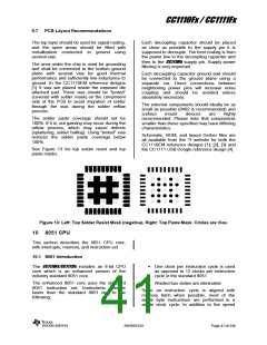
See Figure 13 for top solder resist and top
paste masks.
Figure 13: Left: Top Solder Resist Mask (negative). Right: Top Paste Mask. Circles are Vias.
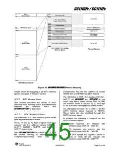
10 8051 CPU
This section describes the 8051 CPU core,
with interrupts, memory, and instruction set.
10.1 8051 Introduction
The CC1110Fx/CC1111Fx includes an 8-bit CPU
core which is an enhanced version of the
industry standard 8051 core.
One clock per instruction cycle is used
as opposed to 12 clocks per instruction
cycle in the standard 8051.
The enhanced 8051 core uses the standard
8051 instruction set. Instructions execute
faster than the standard 8051 due to the
following:
Wasted bus states are eliminated.
Since an instruction cycle is aligned with
memory fetch when possible, most of the
single byte instructions are performed in a
single clock cycle. In addition to the speed
SWRS033H
Page 41 of 246

 TI [ TEXAS INSTRUMENTS ]