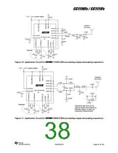
CC1110Fx / CC1111Fx
3.0 V - 3.6 V power supply
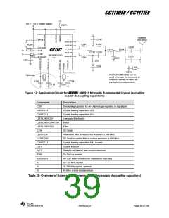
R271
Antenna
(50 Ohm)
C241
L242
4 P1_0
AVDD 26
L241
L231
R264
AVDD 25
RF_N 24
RF_P 23
AVDD 22
C235
2,12 DVDD
R262
L233
L234
CC1111
D+
D-
10 DP
C231 C232
11 DM
DIE ATTACH PAD:
R263
C235'
30 DCOUPL
C233
C301
L232
C234
L235
C236
Alternative filter that can be
used to reduce the emission at
699 MHz below -54 dBm, for
conducted measurements.
Optional:
C181
X2
X3
C203
C214
C171
Figure 12: Application Circuit for CC1111Fx 868/915 MHz with Fundamental Crystal (excluding
supply decoupling capacitors)
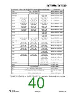
Component
C301
Description
Decoupling capacitor for on-chip voltage regulator to digital part
Crystal loading capacitors (X3)
Crystal loading capacitors (X1)
Low-pass filter/match
C203/C214
C201/C211
L231/L241/C231
L232/L242/C234/C241
L233/L234/C233
C234
Balun
Filter
DC block
L235/C236
C235/C235’
C181/C171
L281
Alternative filter to reduce the emission at 699 MHz
DC block or part of filter to reduce emission at 699 MHz
Crystal loading capacitors if X2 is used.
Crystal inductor
R271
Resistor for internal bias current reference
D+ Pull-up resistor
R264
R262/R263
X1
D+ / D− series resistors for impedance matching
26 - 27 MHz crystal
X2
32.768 kHz crystal, optional
48 MHz crystal (fundamental)
X3
Table 28: Overview of External Components (excluding supply decoupling capacitors)
SWRS033H
Page 39 of 246

 TI [ TEXAS INSTRUMENTS ]