CC1110Fx / CC1111Fx
Total parasitic capacitance is typically 2.5 pF.
to maintain approximately 0.4 Vpp signal
swing. This ensures a fast start-up, and keeps
the drive level to a minimum. The ESR of the
crystal should be within the specification in
order to ensure a reliable start-up
The crystal oscillator is amplitude regulated.
This means that a high current is used to start
up the oscillations. When the amplitude builds
up, the current is reduced to what is necessary
9.4 Reference Signal
The chip can alternatively be operated with a
reference signal from 26 to 27 MHz (CC1110Fx)
or 48 MHz (CC1111Fx) instead of a crystal. This
input clock can either be a full-swing digital
signal (0 V to VDD) or a sine wave of
maximum 1 V peak-peak amplitude. The
reference signal must be connected to the
XOSC_Q1 input. The sine wave must be
connected to XOSC_Q1 using
a
serial
capacitor. When using a full-swing digital
signal this capacitor can be omitted. The
XOSC_Q2 line must be left un-connected. The
crystal loading capacitors and crystal inductor
(if using X4) can be omitted when using a
reference signal
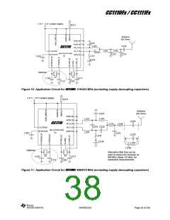
9.5 USB (CC1111Fx)
the pull-up resistor does not provide current to
the D+ line when VBUS is removed. The pull-up
resistor may be connected directly between
VBUS and the D+ line. As an alternative, if the
CC1111Fx firmware needs the ability to
disconnect from the USB bus, an I/O pin on
the CC1111Fx can be used to control the pull-up
resistor.
For the CC1111Fx, the DP and DM pins need
series resistors R262 and R263 for impedance
matching and the D+ line must have a pull-up
resistor, R264. The series resistors should
match the 90
Ω
±15% characteristic
impedance of the USB bus.
Notice that the pull-up resistor must be tied to
a voltage source between 3.0 and 3.6 V
(typically 3.3 V). The voltage source must be
derived from or controlled by the VBUS power
supply provided by the USB cable. In this way,
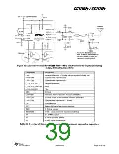
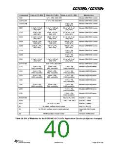
9.6 Power Supply Decoupling
The power supply must be properly decoupled
close to the supply pins. Note that decoupling
capacitors are not shown in the application
circuit. The placement and the size of the
decoupling capacitors are very important to
achieve the optimum performance. TI provides
reference designs that should be followed
closely ([1], [2], [3] and [4]).
SWRS033H
Page 37 of 246

 TI [ TEXAS INSTRUMENTS ]