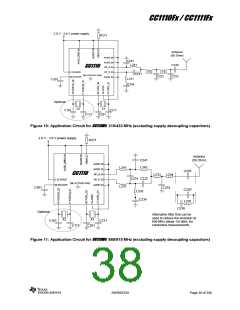
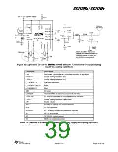
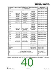
CC1110Fx / CC1111Fx
improvement, the enhanced 8051 core also
includes architectural enhancements:
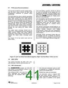
equivalent. However, because the 8051 core
uses a different instruction-timing than many
other 8051 variants, existing code with timing
loops may require modification. Also because
the peripheral units such as timers and serial
ports differ from those on other 8051 cores,
code which includes instructions using the
peripheral units SFRs will not work correctly.
A second data pointer
Extended 18-source interrupt unit
The 8051 core is object code compatible with
the industry standard 8051 microcontroller.
That is, object code compiled with an industry
standard 8051 compiler or assembler
executes on the 8051 core and is functionally
10.2 Memory
The 8051 CPU architecture has four different
memory spaces. The 8051 has separate
memory spaces for program memory and data
memory. The 8051 memory spaces are the
following (see Section 10.2.1 and 10.2.2 for
details):
DMA transfers and hardware debugger
operation.
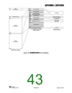
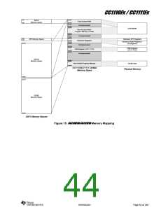
How the different memory spaces are mapped
onto the three physical memories (8/16/32 KB
flash program memory, 1/2/4 KB SRAM, and
hardware registers (SFR, radio, I2S, and USB
(CC1111Fx)) is described in Sections 10.2.1 and
10.2.2.
CODE. A 16-bit read-only memory space for
program memory.
DATA. An 8-bit read/write data memory
space, which can be directly or indirectly,
accessed by a single cycle CPU instruction,
thus allowing fast access. The lower 128 bytes
of the DATA memory space can be addressed
either directly or indirectly, the upper 128 bytes
only indirectly.
10.2.1
Memory Map
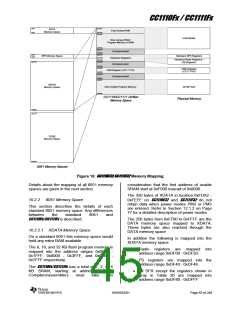
This section gives an overview of the memory
map.
Both the DATA and the SFR memory space is
mapped to the XDATA and CODE memory
space as shown in Figure 14, Figure 15, and
Figure 16 (the CODE and XDATA memory
spaces are mapped identically), and
CC1110FX/CC1111FX has what can be called a
unified memory space.
XDATA. A 16-bit read/write data memory
space, which usually requires 4 - 5 CPU
instruction cycles to access, thus giving slow
access. XDATA assesses is also slower in
hardware than DATA accesses as the CODE
and XDATA memory spaces share a common
bus on the CPU core (instruction pre-fetch
from CODE can not be performed in parallel
with XDATA accesses).
Mapping all the memory spaces to XDATA
allows the DMA controller access to all
physical memory and thus allows DMA
transfers between the different 8051 memory
spaces. This also means that any instruction
that read, write, or manipulate an XDATA
variable can be used on the entire unified
memory space, except writing to or changing
data in flash.
SFR. A 7-bit read/write register memory
space, which can be directly accessed by a
single CPU instruction. For SFRs whose
address is divisible by eight, each bit is also
individually addressable.
Mapping all memory spaces to the CODE
memory space is primarily done to allow
program execution out of the SRAM/XDATA.
The four different memory spaces are distinct
in the 8051 architecture, but are partly
overlapping in the CC1110Fx/CC1111Fx to ease
SWRS033H
Page 42 of 246

 TI [ TEXAS INSTRUMENTS ]