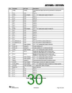
CC1110Fx / CC1111Fx
6.11.1
Filtering of RESET_N pin
The RESET_N pin is sensitive to noise and can cause unintended reset of the chip. For a long reset
line add an external RC filter with values 1 nF and 2.7 k close to the RESET_N pin. When doing
this, note that the RESET_N low width (the shortest pulse that is guaranteed to be recognized as a
reset pin request) is longer than stated in Table 19.
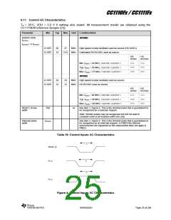
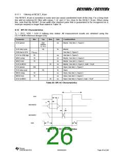
6.12 SPI AC Characteristics
TA = 25 C, VDD = 3.0V if nothing else stated. All measurement results are obtained using the
CC1110EM reference designs ([1]).
Parameter
Min
Typ
Max
Unit
Condition/Note
SCK period
See
ns
Master. See item 1, Figure 5
Section
12.14.3
SCK duty cycle
SSN low to SCK
SCK to SSN high
MISO setup
50
%
Master.
2∙tSYSCLK
30
See item 5, Figure 5
ns
ns
ns
ns
ns
%
See item 6, Figure 5
10
Master. See item 2, Figure 5
Master. See item 3, Figure 5
Master. See item 4, Figure 5, load = 10 pF
Slave. See item 1, Figure 5
Slave.
MISO hold
10
SCK to MOSI
SCK period
25
25
100
SCK duty cycle
MOSI setup
50
10
10
ns
ns
ns
Slave. See item 2, Figure 5
Slave. See item 3, Figure 5
Slave. See item 4, Figure 5, load = 10 pF
MOSI hold
SCK to MISO
Table 20: SPI AC Characteristics
1
SCK
3
2
MISO/MOSI
4
MOSI/MISO
SSN
5
6
Figure 5: SPI AC Characteristics
SWRS033H
Page 26 of 246

 TI [ TEXAS INSTRUMENTS ]