CC1110Fx / CC1111Fx
6.11 Control AC Characteristics
TA = 25 C, VDD = 3.0 V if nothing else stated. All measurement results are obtained using the
CC1110EM reference designs ([1]).
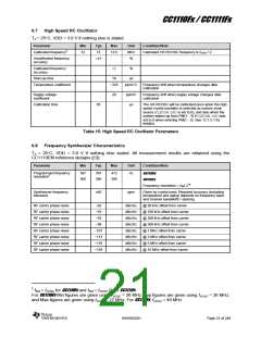
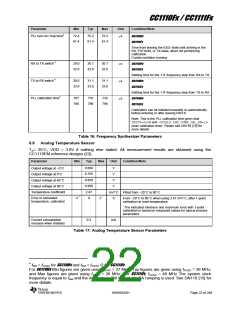
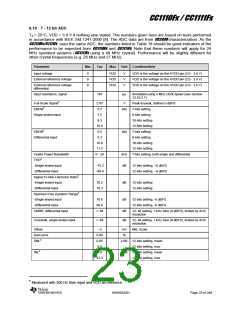
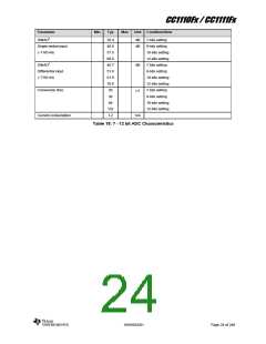
Parameter
Min
Typ
Max
Unit Condition/Note
System clock,
fSYSCLK
CC1110Fx
tSYSCLK= 1/ fSYSCLK
0.1875
0.1875
26
13
27
MHz High speed crystal oscillator used as source (HS XOSC).
MHz Calibrated HS RCOSC used as source.
13.5
HS
HS
XOSC
RCOSC
111
000
000
111
001
001
Min: fXOSC = 24 MHz, CLKCON.CLKSPD=
Typ: fXOSC = 26 MHz, CLKCON.CLKSPD=
Max: fXOSC = 27 MHz, CLKCON.CLKSPD=
CC1111Fx
0.1875
0.1875
24
12
24
12
MHz High speed crystal oscillator used as source
MHz HS RCOSC used as source
HS
HS
XOSC
RCOSC
111
000
000
111
001
001
Min: fXOSC = 48 MHz, CLKCON.CLKSPD=
Typ: fXOSC = 48 MHz, CLKCON.CLKSPD=
Max: fXOSC = 48 MHz, CLKCON.CLKSPD=
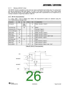
RESET_N low
width
250
ns
See item 1, Figure 4. This is the shortest pulse that is guaranteed to
be recognized as a reset pin request.
Note: Shorter pulses may be recognized but will not lead to
complete reset of all modules within the chip.
Interrupt pulse
width
tSYSCLK
See item 2, Figure 4. This is the shortest pulse that is guaranteed to
be recognized as an interrupt request. In PM2/3 the internal
synchronizers are bypassed so this requirement does not apply in
PM2/3.
Table 19: Control Inputs AC Characteristics
1
RESET_N
Px_n
2
2
Px_n
Figure 4: Control Inputs AC Characteristics
SWRS033H
Page 25 of 246

 TI [ TEXAS INSTRUMENTS ]