CC1110Fx / CC1111Fx
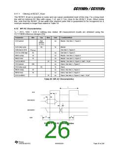
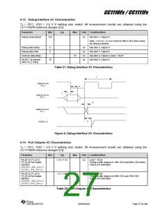
6.13 Debug Interface AC Characteristics
TA = 25 C, VDD = 3.0 V if nothing else stated. All measurement results are obtained using the
CC1110EM reference designs ([1]).
Parameter
Min
Typ
Max
Unit Condition/Note
Debug clock period
125
ns
See item 1, Figure 6
Note: CLKCON.CLKSPDmust be 000 or 001 when using
the debug interface
Debug data setup
Debug data hold
Clock to data delay
5
5
ns
ns
ns
ns
See item 2, Figure 6
See item 3, Figure 6
10
See item 4, Figure 6, load = 10 pF
See item 5, Figure 6
RESET_N inactive
after P2_2 rising
10
Table 21: Debug Interface AC Characteristics
1
DEBUG CLK
P2_2
3
2
DEBUG DATA
P2_1
4
DEBUG DATA
P2_1
5
RESET_N
Figure 6: Debug Interface AC Characteristics
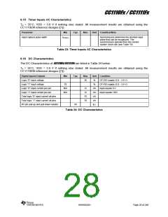
6.14 Port Outputs AC Characteristics
TA = 25 C, VDD = 3.0 V if nothing else stated. All measurement results are obtained using the
CC1110EM reference designs ([1]).
Parameter
Min
Typ
Max
Unit Condition/Note
P0_[0:7], P1_[2:7],
P2_[0:4] Port output
rise time
3.15 / 1.34
ns
Load = 10 pF
Timing is with respect to 10% VDD and 90% VDD levels.
Values are estimated
(IOCFG1.GDO_DS=0/
IOCFG1.GDO_DS=1)
P0_[0:7], P1_[2:7],
P2_[0:4] Port output
fall time
3.2 / 1.44
ns
Load = 10 pF
Timing is with respect to 90% VDD and 10% VDD.
Values are estimated
(IOCFG1.GDO_DS=0/
IOCFG1.GDO_DS=1)
Table 22: Port Outputs AC Characteristics
SWRS033H
Page 27 of 246

 TI [ TEXAS INSTRUMENTS ]