bq51010
bq51011
bq51013
www.ti.com
SLVSAT9B –APRIL 2011–REVISED AUGUST 2011
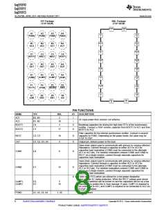
PIN FUNCTIONS (continued)
NAME
YFF
RHL
I/O
DESCRIPTION
I/O
Programming pin for the over current limit. Connect external resistor to
VSS. Size RILIM with the following equation: RILIM = 300 / I( max) where
I(max) is the desired current limit for the power supply.
ILIM
G1
12
Connect this pin to the wired adapter input. When a voltage is applied to
this pin wireless charging is disabled and AD-EN is driven low. Connect to
GND through a 1µF capacitor. If unused, capacitor is not required and
should be grounded directly.
AD
G4
F3
9
8
I
Push-pull driver for external PFET connecting AD and OUT. This node is
pulled to the higher of OUT and AD when turning off the external FET.
This voltage tracks approximately 4V below AD when voltage is present
at AD and provides a regulated VSG bias for the external FET. Float this
pin if unused.
AD-EN
O
Must be connected to ground and pulled up to VTSB via two series
resistors. If an NTC function is not desired, size R2 to be twice that of R3.
As a CTRL pin pull to ground to send End Power/Temperature Fault
message to the transmitter, pull-up to send End Power/Termination
message to the transmitter.
TS/CTRL
F1
13
I
EN1
EN2
G3
G2
10
11
I
I
Inputs that allow user to enable/disable wireless and wired charging <EN1
EN2>
<00> wireless charging is enabled unless the AD voltage is > 3.6 V.
<01> AD mode is disabled, wireless charging enabled.
<10> AD-EN pulled low, wireless charging disabled.
<11> wired and wireless charging disabled.
2.2V LDO that periodically biases the TS/CTRL resistor network. Connect
to TS/CTRL via a resistor
VTSB
CHG
F2
F4
14
7
O
O
Open-drain output – active when output current is being delivered to the
load (i.e. when the output of the supply is enabled).
Spacer
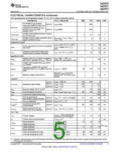
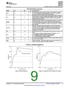
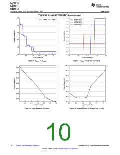
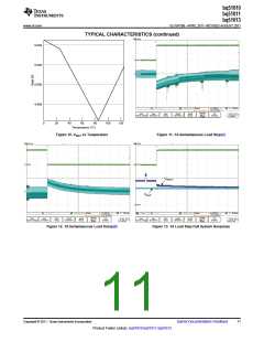
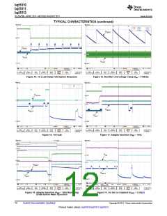
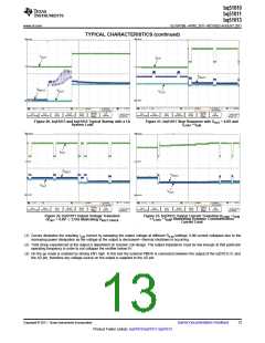
TYPICAL CHARACTERISTICS
100.0
100.0
90.0
80.0
70.0
60.0
90.0
Full Sync Mode Enabled
80.0
70.0
0.0
1.0
2.0
3.0
4.0
5.0
6.0
1.0
2.0
3.0
4.0
5.0
Output Power (W)
Output Power (W)
Figure 4. Rectifier Efficiency
Figure 5. IC Efficiency from AC Input to DC Output
Copyright © 2011, Texas Instruments Incorporated
Submit Documentation Feedback
9
Product Folder Link(s): bq51010 bq51011 bq51013

 TI [ TEXAS INSTRUMENTS ]