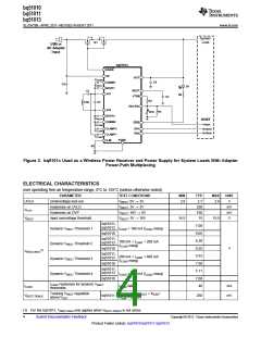
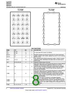
bq51010
bq51011
bq51013
SLVSAT9B –APRIL 2011–REVISED AUGUST 2011
www.ti.com
YFF Package
(TOP VIEW)
RHL Package
(TOP VIEW)
PGND
PGND
20
1
A1
A2
A3
A4
AC1
2
AC2
19
PGND
PGND
PGND
PGND
BOOT1
3
RECT
18
B1
B2
B3
B4
AC2
AC2
AC1
AC1
OUT
4
BOOT2
17
C1
C2
C3
C4
BOOT2
BOOT1
RECT
RECT
CLMP1
5
CLMP2
16
D1
D2
D3
D4
OUT
OUT
OUT
OUT
COM1
6
COM2
15
E1
E2
E3
E4
/CHG
7
VTSB
14
CLMP2
CLMP1
COM2
COM1
TS/
CTRL
13
F1
TS/CTRL
F2
F3
F4
/AD-EN
8
VTSB
AD-EN
CHG
AD
9
ILIM
12
G1
G2
G3
G4
AD
ILIM
EN2
EN1
EN1
10
EN2
11
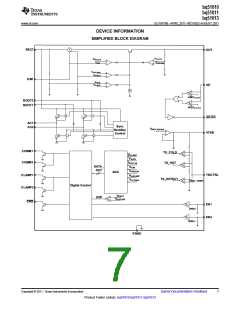
PIN FUNCTIONS
NAME
AC1
YFF
RHL
I/O
DESCRIPTION
B3, B4
B1, B2
C4
2
19
3
I
I
AC input power from receiver coil antenna.
AC2
BOOT1
O
Bootstrap capacitors for driving the high-side FETs of the synchronous
rectifier. Connect a 10nF ceramic capacitor from BOOT1 to AC1 and from
BOOT2 to AC2.
BOOT2
C1
17
O
Filter capacitor for the internal synchronous rectifier. Connect a ceramic
capacitor to PGND. Depending on the power levels, the value may be
4.7μF to 22μF.
RECT
OUT
C2, C3
18
4
O
O
D1, D2, D3, D4
Output pin, delivers power to the load.
Open-drain output used to communicate with primary by varying reflected
impedance. Connect through a capacitor to either AC1 or AC2 for
capacitive load modulation (COM2 must be connected to the alternate
AC1 or AC2 pin). For resistive modulation connect COM1 and COM2 to
RECT via a single resistor; connect through separate capacitors for
capacitive load modulation.
COM1
COM2
E4
E1
6
O
Open-drain output used to communicate with primary by varying reflected
impedance. Connect through a capacitor to either AC1 or AC2 for
capacitive load modulation (COM1 must be connected to the alternate
AC1 or AC2 pin). For resistive modulation connect COM1 and COM2 to
RECT via a single resistor; connect through separate capacitors for
capacitive load modulation.
15
O
O
Open drain FETs which are utilized for a non-power dissipative
over-voltage AC clamp protection. When the RECT voltage goes above
15 V, both switches will be turned on and the capacitors will act as a low
impedance to protect the IC from damage. If used, CLMP1 is required to
be connected to AC1, and CLMP2 is required to be connected to AC2 via
0.47µF capacitors.
CLMP1,
CLMP2
E2,
E3
5
16
PGND
A1, A2, A3, A4
1, 20
Power ground
8
Submit Documentation Feedback
Copyright © 2011, Texas Instruments Incorporated
Product Folder Link(s): bq51010 bq51011 bq51013

 TI [ TEXAS INSTRUMENTS ]