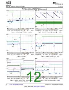
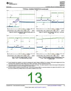
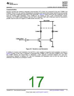
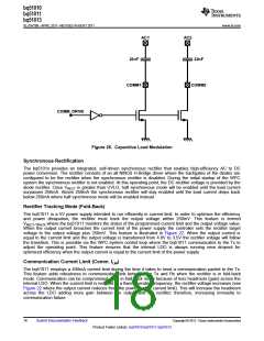
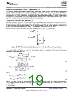
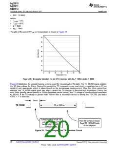
bq51010
bq51011
bq51013
SLVSAT9B –APRIL 2011–REVISED AUGUST 2011
www.ti.com
The EN1 and EN2 pins include internal 200kΩ pull-down resistors, so that if these pins are not connected
bq5101x defaults to AD-EN control mode. However, these pins can be pulled high to enable other operating
modes as described in Table 1:
Table 1.
EN1
EN2
Result
0
0
Adapter control enabled. If adapter is present then secondary charger will
be powered by adapter, otherwise wireless charging will be enabled when
wireless power is available.
0
1
1
1
0
1
Adapter is disabled. Wireless charging will be enabled when wireless
power is present.
AD-EN is pulled low, whether or not adapter voltage is present. This feature
can be used, e.g., for USB OTG applications.
Adapter and wireless charging are disabled, i.e., power will never be
delivered by the OUT pin in this mode.
As described in Table 1, pulling EN2 high disables the adapter mode and only allows wireless charging. In this
mode the adapter voltage will always be blocked from the OUT pin. An application example where this mode is
useful is when USB power is present at AD, but the USB is in suspend mode so that no power can be taken from
the USB supply. Pulling EN1 high enables the off-chip PMOS regardless of the presence of a voltage. This
function can be used in USB OTG mode to allow a charger connected to the OUT pin to power the AD pin.
Finally, pulling both EN1 and EN2 high disables both wired and wireless charging.
NOTE
It is required to connect a back-to-back PMOS between AD and OUT so that voltage is
blocked in both directions. Also, when AD mode is enabled no load can be pulled from the
RECT pin as this could cause an internal device overvoltage in bq5101x.
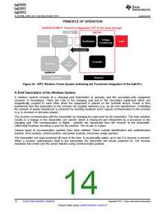
End Power Transfer Packet (WPC Header 0x02)
The WPC allows for a special command for the receiver to terminate power transfer from the trasmitter termed
End Power Transfer (EPT) packet. Table 2 specifies the v1.0 Reasons columb and their responding data field
value. The Condition column corresponds to the values sent by the bq5101x for a given reason.
Table 2.
Reason
Unknown
Value
0x00
0x01
0x02
0x03
0x04
0x05
0x06
0x07
0x08
Condition
AD > 3.6V
TS/CTRL = 1, or EN1 = 1, or <EN1 EN2> = <11>
TJ > 150°C or RILIM < 100Ω
TS < VHOT, TS > VCOLD, or TS/CTRL < 100mV
Not Sent
Charge Complete
Internal Fault
Over Temperature
Over Voltage
Over Current
Battery Failure
Reconfigure
Not Sent
Not Sent
Not Sent
No Response
VRECT target doesn't converge
Status Outputs
bq5101x has one status output, CHG. This output is an open-drain NMOS device that is rated to 20V. The
open-drain FET connected to the CHG pin will be turned on whenever the output of the power supply is enabled.
Please note, the output of the power supply will not be enabled if the VRECT-REG does not converge at the no-load
target voltage.
16
Submit Documentation Feedback
Copyright © 2011, Texas Instruments Incorporated
Product Folder Link(s): bq51010 bq51011 bq51013

 TI [ TEXAS INSTRUMENTS ]