bq51010
bq51011
bq51013
www.ti.com
SLVSAT9B –APRIL 2011–REVISED AUGUST 2011
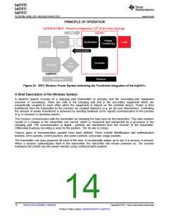
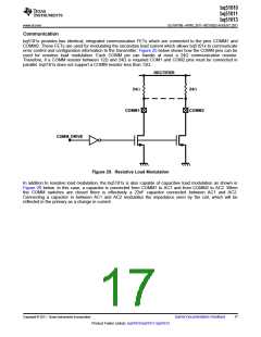
Using the bq5101x as a Wireless Power Supply: (See Figure 3)
Figure 3 is the schematic of a system which uses the bq5101x as power supply while power multiplexing the
wired (adapter) port.
When the system shown in Figure 3 is placed on the charging pad, the receiver coil is inductively coupled to the
magnetic flux generated by the coil in the charging pad which consequently induces a voltage in the receiver coil.
The internal synchronous rectifier feeds this voltage to the RECT pin which has the filter capacitor C3.
The bq5101x identifies and authenticates itself to the primary using the COM pins by switching on and off the
COM FETs and hence switching in and out CCOMM. If the authentication is successful, the transmitter will remain
powered on. The bq5101x measures the voltage at the RECT pin, calculates the difference between the actual
voltage and the desired voltage VRECT-REG, (~7V for the bq51013 at no load) and sends back error packets to the
primary. This process goes on until the input voltage settles at VIN-REG. During a load transient, the dynamic
rectifier algorithm will set the targets specified by VRECT-REG thresholds 1, 2, 3, and 4. This algorithm enhances
the transient response of the power supply.
During power-up, the LDO is held off until the VRECT-REG threshold 1 converges. The voltage control loop ensures
that the output voltage is maintained at VOUT-REG (~5V for the bq51013) to power the system. The bq5101x
meanwhile continues to monitor the input voltage, and maintains sending error packets to the primary every
250ms. If a large transient occurs, the feedback to the primary speeds up to every 32ms in order to converge on
an operating point in less time.
Input Overvoltage
If the input voltage suddenly increases in potential (e.g. a change in position of the equipment on the charging
pad), the voltage-control loop inside the bq5101x becomes active, and prevents the output from going beyond
VOUT-REG. The receiver then starts sending back error packets to the transmitter every 30ms until the input
voltage comes back to the VRECT-REG target, and then maintains the error communication every 250ms.
If the input voltage increases in potential beyond VOVP, the IC switches off the LDO and communicates to the
primary to bring the voltage back to VRECT -REG. In addition, a proprietary voltage protection circuit is activated by
means of CCLAMP1 and CCLAMP2 that protects the IC from voltages beyond the maximum rating of the IC (e.g.
20V).
Adapter Enable Functionality and Enable1/Enable2 Control
Figure 3 is an example application that shows the bq5101x used as a wireless power receiver that can power
mutliplex between wired or wireless power for the down-system electronics. In the default operating mode pins
EN1 and EN2 are low, which activates the adapter enable functionality. In this mode, if an adapter is not present
the AD pin will be low, and AD-EN pin will be pulled to the higher of the OUT and AD pins so that the PMOS
between OUT and AD will be turned off. If an adapter is plugged in and the voltage at the AD pin goes above 3.6
V then wireless charging is disabled and the AD-EN pin will be pulled approximately 4 V below the AD pin to
connect AD to the secondary charger. The difference between AD and AD-EN is regulated to a maximum of 7V
to ensure the VGS of the external PMOS is protected.
Copyright © 2011, Texas Instruments Incorporated
Submit Documentation Feedback
15
Product Folder Link(s): bq51010 bq51011 bq51013

 TI [ TEXAS INSTRUMENTS ]