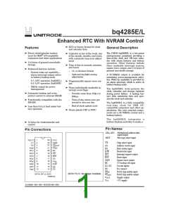
bq4285E/L
Reset may be disabled by connecting RST to
VCC. This allows the control bits to retain their
states through power-down/power-up cycles.
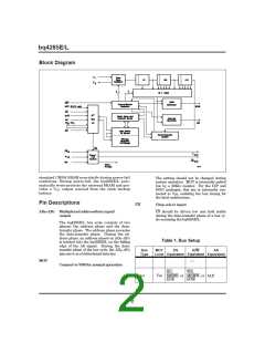
AS
DS
Address strobe input
AS serves to demultiplex the address/data
bus. The falling edge of AS latches the ad-
dress on AD0–AD7. This demultiplexing pro-
cess is independent of the CS signal.
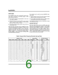
SQW
Square-wave output
SQW may output a programmable fre-
quency square-wave signal during normal
(VCC valid) system operation. Any one of
the 13 specific frequencies may be selected
through register A. This pin is held low
when the square-wave enable bit (SQWE)
in register B is 0 (see the Control/Status
Registers section).
Data strobe input
With MOT = VSS, the DS input is provided a sig-
nal similar to RD, MEMR, or I/OR in an
Intel-based system. The falling edge on DS
is used to enable the outputs during a read
cycle.
A 32.768kHz output is enabled by setting
the SQWE bit in register B to 1 and the
32KE bit in register C to 1 after setting
OSC2–OSC0 in register A to 011 (binary).
BC
3V backup cell input
BC should be connected to a 3V backup cell
for RTC operation and storage register non-
volatility in the absence of power. When VCC
slews down past VBC (3V typical), the inte-
gral control circuitry switches the power
source to BC. When VCC returns above VBC
,
R/W
Read/write input
the power source is switched to VCC
.
Upon power-up, a voltage within the VBC
range must be present on the BC pin for
the oscillator to start up.
With MOT = VSS, R/W is provided a signal simi-
lar to WR, MEMW, or I/OW in an Intel-
based system. The rising edge on R/W
latches data into the bq4285E/L.
X1–X2
Crystal inputs
The X1–X2 inputs are provided for an ex-
ternal 32.768Khz quartz crystal, Daiwa
DT-26 or equivalent, with 6pF load capaci-
tance. A trimming capacitor may be neces-
sary for extremely precise time-base gen-
eration.
INT
Interrupt request output
CEIN
External RAM chip enable input,
active low
INT is an open-drain output. This allows
INT to be valid in battery-backup mode for
the alarm interrupt. To use this feature,
INT must be connected to a power supply
other than VCC. INT is asserted low when
any event flag is set and the corresponding
event enable bit is also set. INT becomes
high-impedance whenever register C is read
(see the Control/Status Registers section).
CEIN should be driven low to enable the
controlled external RAM. CEIN is internally
pulled up with a 50KΩ resistor.
CEOUT
External RAM chip enable output,
active low
When power is valid, CEOUT reflects CEIN.
RST
Reset input
VOUT
Supply output
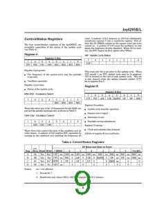
The bq4285E/L is reset when RST is pulled
low. When reset, INT becomes high-
impedance, and the bq4285E/L is not accessi-
ble. Table 4 in the Control/Status Registers
section lists the register bits that are cleared
by a reset.
VOUT provides the higher of VCC or VBC
,
switched internally, to supply external RAM.
VCC
VSS
Positive power supply
Ground
3

 TI [ TEXAS INSTRUMENTS ]