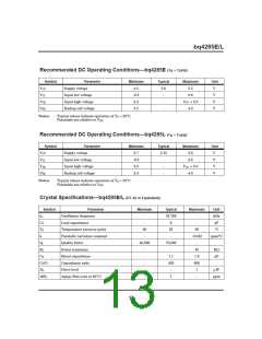
bq4285E/L
vider. A pattern of 011 behaves as 010 but additionally
transforms register C into a read/write register. This al-
lows the 32.768kHz output on the square wave pin to be
turned on. A pattern of 11X turns the oscillator on, but
keeps the frequency divider disabled. When 010 is writ-
ten, the RTC begins its first update after 500ms.
Control/Status Registers
The four control/status registers of the bq4285E/L are
accessible regardless of the status of the update cycle
(see Table 4).
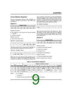
Register A
UIP - Update Cycle Status
Register A Bits
7
6
-
5
-
4
-
3
-
2
-
1
-
0
-
7
6
5
4
3
2
1
0
UIP
UIP OS2 OS1 OS0 RS3 RS2 RS1 RS0
Register A programs:
This read-only bit is set prior to the update cycle. When
UIP equals 1, an RTC update cycle may be in progress.
UIP is cleared at the end of each update cycle. This bit
is also cleared when the update transfer inhibit (UTI)
bit in register B is 1.
n
n
The frequency of the square-wave and the periodic
event rate.
Oscillator operation.
Register A provides:
Status of the update cycle.
Register B
n
Register B Bits
RS0–RS3 - Frequency Select
7
6
5
4
3
2
1
0
UTI PIE AIE UIE SQWE DF
HF DSE
7
-
6
-
5
-
4
-
3
2
1
0
RS3 RS2 RS1 RS0
Register B enables:
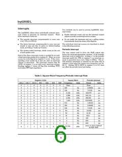
These bits select one of the 13 frequencies for the SQW out-
put and the periodic interrupt rate, as shown in Table 3.
n
n
n
n
Update cycle transfer operation
Square-wave output
OS0–OS2 - Oscillator Control
Interrupt events
Daylight saving adjustment
7
-
6
5
4
3
-
2
-
1
-
0
-
OS2 OS1 OS0
Register B selects:
Clock and calendar data formats
All bits of register B are read/write.
n
These three bits control the state of the oscillator and di-
vider stages. A pattern of 010 enables RTC operation by
turning on the oscillator and enabling the frequency di-
Table 4. Control/Status Registers
Bit Name and State on Reset
Loc.
Reg. (Hex) Read Write 7 (MSB)
6
5
4
3
2
1
0 (LSB)
A
B
C
D
0A
0B
0C
0D
Yes Yes1 UIP na OS2 na OS1 na OS0 na RS3 na RS2 na RS1 na RS0 na
Yes
Yes No2 INTF
Yes No VRT na
Yes UTI na PIE
0
0
0
AIE
AF
-
0
0
0
UIE
UF
-
0
0
0
SQWE
0
0
0
DF na HF na DSE na
0
PF
-
-
-
32KE na
-
-
0
0
-
-
0
0
-
0
Notes:
na = not affected.
1. Except bit 7.
2. Read/write only when OSC2–OSC0 in register A is 011 (binary).
9

 TI [ TEXAS INSTRUMENTS ]