bq4285E/L
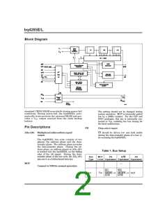
Block Diagram
standard CMOS SRAM nonvolatile during power-fail
conditions. During power-fail, the bq4285E/L auto-
matically write-protects the external SRAM and pro-
vides a VCC output sourced from the clock backup
battery.
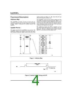
The setting should not be changed during
system operation. MOT is internally pulled
low by a 20KΩ resistor. For the DIP and
SOIC packages, this pin is internally con-
nected to VSS, enabling the bus timing for
the Intel architecture.
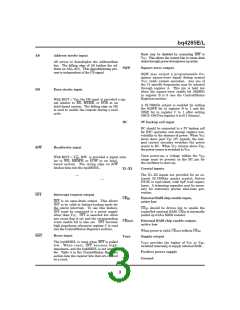
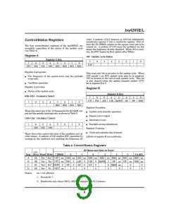
Pin Descriptions
CS
Chip select input
AD0–AD7 Multiplexed address/data input/
output
CS should be driven low and held stable
during the data-transfer phase of a bus cy-
cle accessing the bq4285E/L.
The bq4285E/L bus cycle consists of two
phases: the address phase and the data-
transfer phase. The address phase precedes
the data-transfer phase. During the ad-
dress phase, an address placed on AD0–AD7
is latched into the bq4285E/L on the falling
edge of the AS signal. During the data-
transfer phase of the bus cycle, the AD0–AD7
pins serve as a bidirectional data bus.
Table 1. Bus Setup
Bus
Type
MOT
DS
R/W
AS
Level Equivalent Equivalent Equivalent
MOT
Connect to VSS for normal operation
RD,
MEMR, or MEMW, or ALE
I/OR I/OW
WR,
VSS
Intel
2

 TI [ TEXAS INSTRUMENTS ]