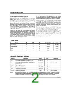
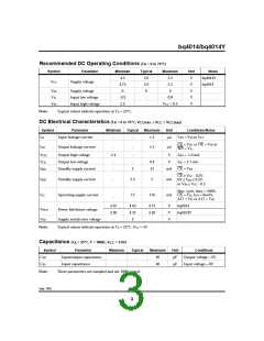
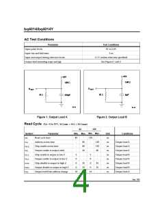
bq4014/bq4014Y
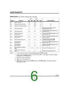
Write Cycle (T = 0 to 70°C, V
≤ V
≤ V
)
CCmax
A
CCmin
CC
-120
-85
Min. Max.
Min. Max.
Symbol
tWC
Parameter
Write cycle time
Units
ns
Conditions/Notes
85
75
75
-
-
-
120
100
100
-
-
-
tCW
Chip enable to end of write
Address valid to end of write
ns
(1)
(1)
tAW
ns
Measured from address valid to
beginning of write. (2)
tAS
Address setup time
Write pulse width
0
65
5
-
-
0
85
5
-
-
ns
ns
ns
ns
ns
ns
ns
ns
ns
Measured from beginning of write to
end of write. (1)
tWP
Write recovery time
(write cycle 1)
Measured from WE going high to end
of write cycle. (3)
tWR1
tWR2
tDW
tDH1
tDH2
tWZ
-
-
Write recovery time
(write cycle 2)
Measured from CE going high to end
of write cycle. (3)
15
35
0
-
15
45
0
-
Measured to first low-to-high
transition of either CE or WE.
Data valid to end of write
-
-
Data hold time
(write cycle 1)
Measured from WE going high to end
of write cycle. (4)
-
-
Data hold time
(write cycle 2)
Measured from CE going high to end
of write cycle. (4)
10
0
-
10
0
-
Write enabled to output in
high Z
30
-
40
-
I/O pins are in output state. (5)
I/O pins are in output state. (5)
Output active from end of
write
tOW
0
0
Notes:
1. A write ends at the earlier transition of CE going high and WE going high.
2. A write occurs during the overlap of a low CE and a low WE. A write begins at the later transition
of CE going low and WE going low.
3. Either tWR1 or tWR2 must be met.
4. Either tDH1 or tDH2 must be met.
5. If CE goes low simultaneously with WE going low or after WE going low, the outputs remain in
high-impedance state.
Sept. 1992
6

 TI [ TEXAS INSTRUMENTS ]