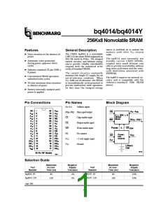
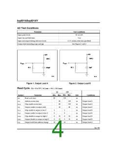
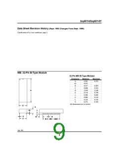
bq4014/bq4014Y
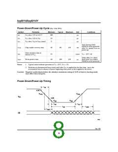
As VCC falls past VPFD and approaches 3V, the control
circuitry switches to the internal lithium backup supply,
which provides data retention until valid VCC is applied.
Functional Description
When power is valid, the bq4014 operates as a standard
CMOS SRAM. During power-down and power-up cycles,
the bq4014 acts as a nonvolatile memory, automatically
protecting and preserving the memory contents.
When VCC returns to a level above the internal backup
cell voltage, the supply is switched back to VCC
. After
VCC ramps above the VPFD threshold, write-protection
continues for a time tCER (120ms maximum) to allow for
processor stabilization. Normal memory operation may
resume after this time.
P ower -down /power -u p con t r ol cir cu it r y con sta n tly
monitors the VCC supply for a power-fail-detect threshold
VPFD. The bq4014 monitors for VPFD = 4.62V typical for
use in systems with 5% supply tolerance. The bq4014Y
monitors for VPFD = 4.37V typical for use in systems with
10% supply tolerance.
The internal coin cells used by the bq4014 have an
extremely long shelf life and provide data retention for
more than 10 years in the absence of system power.
When VCC falls below the VPFD threshold, the SRAM
a utom a tica lly wr ite-pr otects the data . All outputs
become high impedance, and all inputs are treated as
“don’t care.” If a valid access is in process at the time of
power-fail detection, the memory cycle continues to com-
pletion. If the memory cycle fails to terminate within
time tWPT, write-protection takes place.
As shipped from Benchmarq, the integral lithium cells
are electrically isolated from the memory. (Self-discharge
in t his con dition is a ppr oxim ately 0.5% per yea r .)
Following the first application of VCC, this isolation is
broken, and the lithium backup provides data retention
on subsequent power-downs.
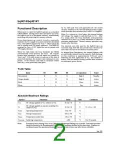
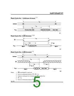
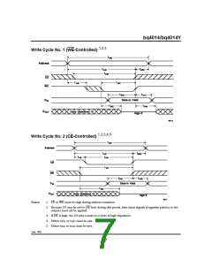
Truth Table
Mode
Not selected
CE
H
L
WE
X
OE
X
I/O Operation
High Z
High Z
DOUT
Power
Standby
Active
Output disable
Read
H
H
L
H
L
Active
Write
L
L
X
DIN
Active
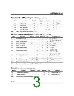
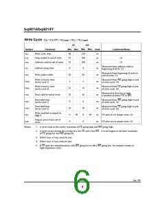
Absolute Maximum Ratings
Symbol
Parameter
Value
Unit
Conditions
VCC
DC voltage applied on VCC relative to VSS
-0.3 to 7.0
V
DC voltage applied on any pin excluding VCC
relative to VSS
VT
-0.3 to 7.0
V
VT ≤ VCC + 0.3
TOPR
TSTG
TBIAS
Operating temperature
Storage temperature
Temperature under bias
0 to +70
-40 to +70
-10 to +70
+260
°C
°C
°C
°C
TSOLDER Soldering temperature
For 10 seconds
Note:
Permanent device damage may occur if Absolu te Ma xim u m Ratin gs are exceeded. Functional operation
should be limited to the Recommended DC Operating Conditions detailed in this data sheet. Exposure to
conditions beyond the operational limits for extended periods of time may affect device reliability.
Sept. 1992
2

 TI [ TEXAS INSTRUMENTS ]