bq4014/bq4014Y
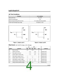
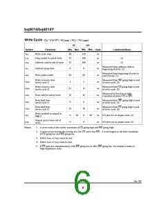
AC Test Conditions
Parameter
Test Conditions
0V to 3.0V
Input pulse levels
Input rise and fall times
5 ns
Input and output timing reference levels
Output load (including scope and jig)
1.5 V (unless otherwise specified)
See Figures 1 and 2
Figure 1. Output Load A
Figure 2. Output Load B
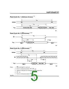
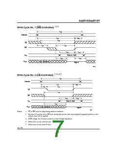
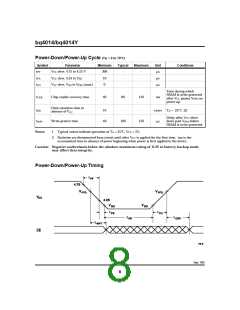
Read Cycle (T = 0 to 70°C, V
≤ V
≤ V
)
CCmax
A
CCmin
CC
-120
Min. Max.
-85
Min. Max.
Symbol
tRC
Parameter
Unit
ns
ns
ns
ns
ns
ns
ns
ns
ns
Conditions
Read cycle time
85
-
-
85
85
45
-
120
-
-
120
120
60
-
tAA
Address access time
Chip enable access time
Output load A
tACE
tOE
-
-
Output load A
Output load A
Output load B
Output load B
Output load B
Output load B
Output load A
Output enable to output valid
Chip enable to output in low Z
Output enable to output in low Z
Chip disable to output in high Z
Output disable to output in high Z
Output hold from address change
-
-
tCLZ
tOLZ
tCHZ
tOHZ
tOH
5
5
0
-
0
-
0
35
25
-
0
45
35
-
0
0
10
10
Sept. 1992
4

 TI [ TEXAS INSTRUMENTS ]