bq24735
SLUSAK9 –SEPTEMBER 2011
www.ti.com
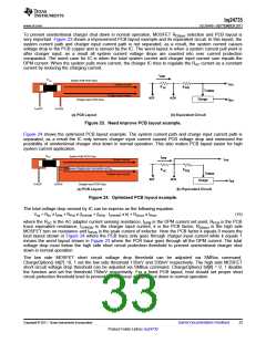
PCB Layout
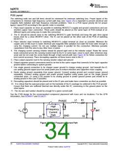
The switching node rise and fall times should be minimized for minimum switching loss. Proper layout of the
components to minimize high frequency current path loop (see Figure 25) is important to prevent electrical and
magnetic field radiation and high frequency resonant problems. Here is a PCB layout priority list for proper
layout. Layout PCB according to this specific order is essential.
1. Place input capacitor as close as possible to switching MOSFET’s supply and ground connections and use
shortest copper trace connection. These parts should be placed on the same layer of PCB instead of on
different layers and using vias to make this connection.
2. The IC should be placed close to the switching MOSFET’s gate terminals and keep the gate drive signal
traces short for a clean MOSFET drive. The IC can be placed on the other side of the PCB of switching
MOSFETs.
3. Place inductor input terminal to switching MOSFET’s output terminal as close as possible. Minimize the
copper area of this trace to lower electrical and magnetic field radiation but make the trace wide enough to
carry the charging current. Do not use multiple layers in parallel for this connection. Minimize parasitic
capacitance from this area to any other trace or plane.
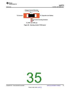
4. The charging current sensing resistor should be placed right next to the inductor output. Route the sense
leads connected across the sensing resistor back to the IC in same layer, close to each other (minimize loop
area) and do not route the sense leads through a high-current path (see Figure 26 for Kelvin connection for
best current accuracy). Place decoupling capacitor on these traces next to the IC
5. Place output capacitor next to the sensing resistor output and ground
6. Output capacitor ground connections need to be tied to the same copper that connects to the input capacitor
ground before connecting to system ground.
7. Use single ground connection to tie charger power ground to charger analog ground. Just beneath the IC
use analog ground copper pour but avoid power pins to reduce inductive and capacitive noise coupling
8. Route analog ground separately from power ground. Connect analog ground and connect power ground
separately. Connect analog ground and power ground together using power pad as the single ground
connection point. Or using a 0Ω resistor to tie analog ground to power ground (power pad should tie to
analog ground in this case if possible).
9. Decoupling capacitors should be placed next to the IC pins and make trace connection as short as possible
10. It is critical that the exposed power pad on the backside of the IC package be soldered to the PCB ground.
Ensure that there are sufficient thermal vias directly under the IC, connecting to the ground plane on the
other layers.
11. The via size and number should be enough for a given current path.
See the EVM design for the recommended component placement with trace and via locations. For the QFN
information, See SCBA017 and SLUA271.
R1
L1
VBAT
PHASE
High
Frequency
Current
Path
VIN
BAT
GND
C2
C1
Figure 25. High Frequency Current Path
34
Submit Documentation Feedback
Copyright © 2011, Texas Instruments Incorporated
Product Folder Link(s) :bq24735

 TI [ TEXAS INSTRUMENTS ]