bq24735
SLUSAK9 –SEPTEMBER 2011
www.ti.com
DETAILED DESCRIPTION
SMBus Interface
The bq24735 operates as a slave, receiving control inputs from the embedded controller host through the SMBus
interface. The bq24735 uses a simplified subset of the commands documented in System Management Bus
Specification V1.1, which can be downloaded from www.smbus.org. The bq24735 uses the SMBus Read-Word
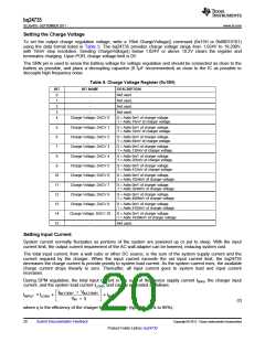
and Write-Word protocols (see Figure 18) to communicate with the smart battery. The bq24735 performs only as
a SMBus slave device with address 0b00010010 (0x12H) and does not initiate communication on the bus. In
addition, the bq24735 has two identification registers a 16-bit device ID register (0xFFH) and a 16-bit
manufacturer ID register (0xFEH).
SMBus communication is enabled with the following conditions:
•
•
VVCC is above UVLO;
VACDET is above 0.6V;
The data (SDA) and clock (SCL) pins have Schmitt-trigger inputs that can accommodate slow edges. Choose
pull-up resistors (10kΩ) for SDA and SCL to achieve rise times according to the SMBus specifications.
Communication starts when the master signals a START condition, which is a high-to-low transition on SDA,
while SCL is high. When the master has finished communicating, the master issues a STOP condition, which is a
low-to-high transition on SDA, while SCL is high. The bus is then free for another transmission. Figure 19 and
Figure 20 show the timing diagram for signals on the SMBus interface. The address byte, command byte, and
data bytes are transmitted between the START and STOP conditions. The SDA state changes only while SCL is
low, except for the START and STOP conditions. Data is transmitted in 8-bit bytes and is sampled on the rising
edge of SCL. Nine clock cycles are required to transfer each byte in or out of the bq24735 because either the
master or the slave acknowledges the receipt of the correct byte during the ninth clock cycle. The bq24735
supports the charger commands as described in Table 2.
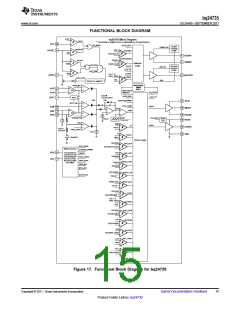
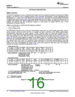
a) Write-Word Format
SLAVE
ADDRESS
COMMAND
BYTE
LOW DATA
BYTE
HIGH DATA
BYTE
S
W
ACK
ACK
ACK
ACK
P
7 BITS
1b
0
1b
0
8 BITS
1b
0
8 BITS
1b
0
8 BITS
1b
0
MSB LSB
MSB LSB
MSB LSB
MSB LSB
Preset to 0b0001001 ChargeCurrent() = 0x14H D7
ChargeVoltage() = 0x15H
InputCurrent() = 0x3FH
D0
D15
D8
ChargeOption() = 0x12H
b) Read-Word Format
SLAVE
ADDRESS
COMMAND
BYTE
SLAVE
ADDRESS
LOW DATA
BYTE
HIGH DATA
BYTE
S
W
ACK
ACK
S
R
ACK
ACK
NACK
P
7 BITS
1b
0
1b
0
8 BITS
1b
0
7 BITS
1b
1
1b
0
8 BITS
1b
0
8 BITS
1b
1
MSB LSB
MSB LSB
MSB LSB
MSB LSB
MSB
LSB
Preset to 0b0001001
DeviceID() = 0xFFH
Preset to
0b0001001
D7 D0
D15 D8
ManufactureID() = 0xFEH
ChargeCurrent() = 0x14H
ChargeVoltage() = 0x15H
InputCurrent() = 0x3FH
ChargeOption() = 0x12H
LEGEND:
S = START CONDITION OR REPEATED START CONDITION
ACK = ACKNOWLEDGE (LOGIC-LOW)
W = WRITE BIT (LOGIC-LOW)
P = STOP CONDITION
NACK = NOT ACKNOWLEDGE (LOGIC-HIGH)
R = READ BIT (LOGIC-HIGH)
MASTER TO SLAVE
SLAVE TO MASTER
Figure 18. SMBus Write-Word and Read-Word Protocols
16
Submit Documentation Feedback
Copyright © 2011, Texas Instruments Incorporated
Product Folder Link(s) :bq24735

 TI [ TEXAS INSTRUMENTS ]