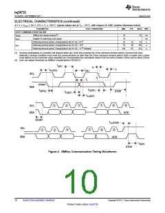
bq24735
SLUSAK9 –SEPTEMBER 2011
www.ti.com
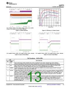
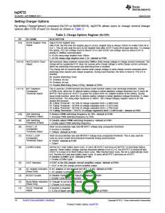
Pin Functions – 20-Pin QFN (continued)
PIN
DESCRIPTION
NO. NAME
6
ACDET
Adapter detection input. Program adapter valid input threshold by connecting a resistor divider from adapter input to
ACDET pin to GND pin. When ACDET pin is above 0.6V and VCC is above UVLO, REGN LDO is present, ACOK
comparator and IOUT are both active.
7
IOUT
Buffered adapter or charge current output, selectable with SMBus command ChargeOption(). IOUT voltage is 20 times
the differential voltage across sense resistor. Place a 100pF or less ceramic decoupling capacitor from IOUT pin to
GND.
8
9
SDA
SCL
ILIM
SMBus open-drain data I/O. Connect to SMBus data line from the host controller or smart battery. Connect a 10kΩ
pull-up resistor according to SMBus specifications.
SMBus open-drain clock input. Connect to SMBus clock line from the host controller or smart battery. Connect a 10kΩ
pull-up resistor according to SMBus specifications.
10
Charge current limit input. Program ILIM voltage by connecting a resistor divider from system reference 3.3V rail to ILIM
pin to GND pin. The lower of ILIM voltage or DAC limit voltage sets charge current regulation limit. To disable the
control on ILIM, set ILIM above 1.6V. Once voltage on ILIM pin falls below 75mV, charge (buck mode) or discharge
(boost mode) is disabled. Charge and discharge is enabled when ILIM pin rises above 105mV.
11
12
BATDRV Charge pump output to drive Battery to System n-channel MOSFET (BATFET). BATDRV voltage is 6V above SRN to
turn on BATFET to power the system from battery. BATDRV voltage is SRN voltage to turn off BATFET to power
system from AC adapter. Place a 4kΩ resistor from BATDRV to the gate of BATFET limits the in-rush current on
BATDRV pin.
SRN
Charge current sense resistor negative input. SRN pin is for battery voltage sensing as well. Connect SRN pin to a 7.5
Ω resistor first then from resistor another terminal connect a 0.1µF ceramic capacitor to GND for common-mode filtering
and connect to current sensing resistor. Connect a 0.1µF ceramic capacitor between current sensing resistor to provide
differential mode filtering. See application information about negative output voltage protection for hard shorts on battery
to ground or battery reverse connection by adding small resistor.
13
14
SRP
GND
Charge current sense resistor positive input. Connect SRP pin to a 10 Ω resistor first then from resistor another terminal
connect to current sensing resistor. Connect a 0.1µF ceramic capacitor between current sensing resistor to provide
differential mode filtering. See application information about negative output voltage protection for hard shorts on battery
to ground or battery reverse connection by adding small resistor.
IC ground. On PCB layout, connect to analog ground plane, and only connect to power ground plane through the power
pad underneath IC.
15
16
LODRV
REGN
Low side power MOSFET driver output. Connect to low side n-channel MOSFET gate.
Linear regulator output. REGN is the output of the 6V linear regulator supplied from VCC. The LDO is active when
voltage on ACDET pin is above 0.6V and voltage on VCC is above UVLO. Connect a 1µF ceramic capacitor from
REGN to GND.
17
BTST
High side power MOSFET driver power supply. Connect a 0.047µF capacitor from BTST to PHASE, and a bootstrap
Schottky diode from REGN to BTST.
18
19
20
HIDRV
PHASE
VCC
High side power MOSFET driver output. Connect to the high side n-channel MOSFET gate.
High side power MOSFET driver source. Connect to the source of the high side n-channel MOSFET.
Input supply, diode OR from adapter or battery voltage. Use 10Ω resistor and 1µF capacitor to ground as low pass filter
to limit inrush current.
PowerPAD
Exposed pad beneath the IC. Analog ground and power ground star-connected only at the PowerPad plane. Always
solder PowerPad to the board, and have vias on the PowerPad plane connecting to analog ground and power ground
planes. It also serves as a thermal pad to dissipate the heat.
14
Submit Documentation Feedback
Copyright © 2011, Texas Instruments Incorporated
Product Folder Link(s) :bq24735

 TI [ TEXAS INSTRUMENTS ]