bq24707
bq24707A
www.ti.com
SLUSA78B –JULY 2010–REVISED MARCH 2011
The lower the FOM value, the lower the total power loss. Usually lower RDS(ON) has higher cost with the same
package size.
The top-side MOSFET loss includes conduction loss and switching loss. It is a function of duty cycle
(D=VOUT/VIN), charging current (ICHG), MOSFET's on-resistance ®DS(ON)), input voltage (VIN), switching frequency
(fS), turn on time (ton) and turn off time (toff):
1
2
= D ´ ICHG ´ RDS(on)
P
+
´ V ´ ICHG ´ (ton + toff ) ´ fs
IN
top
2
(9)
The first item represents the conduction loss. Usually MOSFET RDS(ON) increases by 50% with 100°C junction
temperature rise. The second term represents the switching loss. The MOSFET turn-on and turn-off times are
given by:
QSW
QSW
ton
=
, toff =
Ion
Ioff
(10)
where Qsw is the switching charge, Ion is the turn-on gate driving current and Ioff is the turn-off gate driving
current. If the switching charge is not given in MOSFET datasheet, it can be estimated by gate-to-drain charge
(QGD) and gate-to-source charge (QGS):
1
QSW = QGD
+
´ QGS
2
(11)
Gate driving current can be estimated by REGN voltage (VREGN), MOSFET plateau voltage (Vplt), total turn-on
gate resistance (Ron) and turn-off gate resistance (Roff) of the gate driver:
VREGN - Vplt
Vplt
Ion
=
, Ioff =
Ron
Roff
(12)
The conduction loss of the bottom-side MOSFET is calculated with the following equation when it operates in
synchronous continuous conduction mode:
P
= (1 - D) ´ ICHG2 ´ RDS(on)
bottom
(13)
When charger operates in non-synchronous mode, the bottom-side MOSFET is off. As a result all the
freewheeling current goes through the body-diode of the bottom-side MOSFET. The body diode power loss
depends on its forward voltage drop (VF), non-synchronous mode charging current (INONSYNC), and duty cycle (D).
PD = VF x INONSYNC x (1 - D)
(14)
The maximum charging current in non-synchronous mode can be up to 0.25A for a 10mΩ charging current
sensing resistor or 0.5A if battery voltage is below 2.5V. The minimum duty cycle happens at lowest battery
voltage. Choose the bottom-side MOSFET with either an internal Schottky or body diode capable of carrying the
maximum non-synchronous mode charging current.
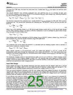
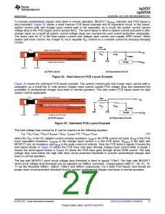
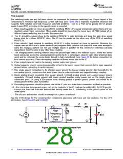
Input Filter Design
During adapter hot plug-in, the parasitic inductance and input capacitor from the adapter cable form a second
order system. The voltage spike at VCC pin maybe beyond IC maximum voltage rating and damage IC. The
input filter must be carefully designed and tested to prevent over voltage event on VCC pin.
There are several methods to damping or limit the over voltage spike during adapter hot plug-in. An electrolytic
capacitor with high ESR as an input capacitor can damp the over voltage spike well below the IC maximum pin
voltage rating. A high current capability TVS Zener diode can also limit the over voltage level to an IC safe level.
However these two solutions may not have low cost or small size.
A cost effective and small size solution is shown in Figure 20. The R1 and C1 are composed of a damping RC
network to damp the hot plug-in oscillation. As a result the over voltage spike is limited to a safe level. D1 is used
for reverse voltage protection for VCC pin. C2 is VCC pin decoupling capacitor and it should be place to VCC pin
as close as possible. C2 value should be less than C1 value so R1 can dominant the equivalent ESR value to
get enough damping effect. R2 is used to limit inrush current of D1 to prevent D1 getting damage when adapter
hot plug-in. R2 and C2 should have 10us time constant to limit the dv/dt on VCC pin to reduce inrush current
when adapter hot plug in. R1 has high inrush current. R1 package must be sized enough to handle inrush current
power loss according to resistor manufacturer’s datasheet. The filter components value always need to be
verified with real application and minor adjustments may need to fit in the real application circuit.
© 2010–2011, Texas Instruments Incorporated
Submit Documentation Feedback
25
Product Folder Link(s): bq24707 bq24707A

 TI [ TEXAS INSTRUMENTS ]