bq24707
bq24707A
SLUSA78B –JULY 2010–REVISED MARCH 2011
www.ti.com
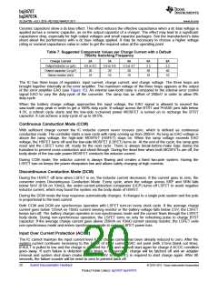
The maximum inductor ripple current happens with D = 0.5 or close to 0.5. For example, the battery charging
voltage range is from 9V to 12.6V for 3-cell battery pack. For 20V adapter voltage, 10V battery voltage gives the
maximum inductor ripple current. Another example is 4-cell battery, the battery voltage range is from 12V to
16.8V, and 12V battery voltage gives the maximum inductor ripple current.
Usually inductor ripple is designed in the range of (20-40%) maximum charging current as a trade-off between
inductor size and efficiency for a practical design.
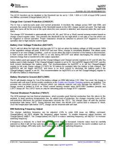
The IC has charge under current protection (UCP) by monitoring charging current sensing resistor cycle-by-cycle.
The typical cycle-by-cycle UCP threshold is 5mV falling edge corresponding to 0.5A falling edge for a 10mΩ
charging current sensing resistor. When the average charging current is less than 125mA for a 10mΩ charging
current sensing resistor, the low side MOSFET is off until BTST capacitor voltage needs to refresh charge. As a
result, the converter relies on low side MOSFET body diode for the inductor freewheeling current.
Input Capacitor
Input capacitor should have enough ripple current rating to absorb input switching ripple current. The worst case
RMS ripple current is half of the charging current when duty cycle is 0.5. If the converter does not operate at
50% duty cycle, then the worst case capacitor RMS current occurs where the duty cycle is closest to 50% and
can be estimated by Equation 6:
ICIN = ICHG
´
D × (1 - D)
(6)
Low ESR ceramic capacitor such as X7R or X5R is preferred for input decoupling capacitor and should be
placed to the drain of the high side MOSFET and source of the low side MOSFET as close as possible. Voltage
rating of the capacitor must be higher than normal input voltage level. 25V rating or higher capacitor is preferred
for 19-20V input voltage. 10-20μF capacitance is suggested for typical of 3-4A charging current.
Ceramic capacitors show a dc-bias effect. This effect reduces the effective capacitance when a dc-bias voltage is
applied across a ceramic capacitor, as on the input capacitor of a charger. The effect may lead to a significant
capacitance drop, especially for high input voltages and small capacitor packages. See the manufacturer's data
sheet about the performance with a dc bias voltage applied. It may be necessary to choose a higher voltage
rating or nominal capacitance value in order to get the required value at the operating point.
Output Capacitor
Output capacitor also should have enough ripple current rating to absorb output switching ripple current. The
output capacitor RMS current is given:
IRIPPLE
ICOUT
=
» 0.29 ´ IRIPPLE
2 ´
3
(7)
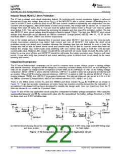
The IC has internal loop compensator. To get good loop stability, the resonant frequency of the output inductor
and output capacitor should be designed between 10 kHz and 20 kHz. The preferred ceramic capacitor is 25V
X7R or X5R for output capacitor. 10-20μF capacitance is suggested for typical of 3-4A charging current. Place
capacitors after charging current sensing resistor to get the best charge current regulation accuracy.
Ceramic capacitors show a dc-bias effect. This effect reduces the effective capacitance when a dc-bias voltage is
applied across a ceramic capacitor, as on the output capacitor of a charger. The effect may lead to a significant
capacitance drop, especially for high output voltages and small capacitor packages. See the manufacturer's data
sheet about the performance with a dc bias voltage applied. It may be necessary to choose a higher voltage
rating or nominal capacitance value in order to get the required value at the operating point.
Power MOSFETs Selection
Two external N-channel MOSFETs are used for a synchronous switching battery charger. The gate drivers are
internally integrated into the IC with 6V of gate drive voltage. 30V or higher voltage rating MOSFETs are
preferred for 19-20V input voltage.
Figure-of-merit (FOM) is usually used for selecting proper MOSFET based on a tradeoff between the conduction
loss and switching loss. For top side MOSFET, FOM is defined as the product of a MOSFET's on-resistance,
RDS(ON), and the gate-to-drain charge, QGD. For bottom side MOSFET, FOM is defined as the product of the
MOSFET's on-resistance, RDS(ON), and the total gate charge, QG.
FOMtop = RDS(on) x QGD; FOMbottom = RDS(on) x QG
(8)
24
Submit Documentation Feedback
© 2010–2011, Texas Instruments Incorporated
Product Folder Link(s): bq24707 bq24707A

 TI [ TEXAS INSTRUMENTS ]