ꢀ ꢁꢂ ꢃ ꢄ ꢅ ꢂ ꢆ ꢀꢁ ꢂꢃ ꢄꢅ ꢇ
SLUS553D − MAY 2003 − REVISED JULY 2005
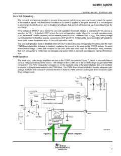
Zero Volt Operating
The zero volt operation is intended to provide a low current path to close open packs and protect the system
in the event of a pack cell short-circuit condition or if a short is applied to the pack terminal. It is not designed
to precharge depleted packs, as it is disabled at voltages that are not within normal pack operating range for
precharge.
If the voltage at BATDEP pin is below the zero volt operation threshold , charge is enabled (EN=HI), and ac is
selected (ACSEL=HI) the bq24702/3 enters the zero volt operation mode. When the zero volt operation mode
is on, the internal PWM is disabled, and an internal power MOSFET connects SRP to V . The battery charge
CC
current is limited by the filter resistor connected to SRP pin (R19). R19 must be dimensioned to withstand the
worst case power dissipation when in zero volt operation mode.
The zero volt operation mode is disabled when BATDEP is above the zero volt operation threshold, and the main
PWM loop is turned on if charge is enabled, regulating the current to the value set by SRSET voltage. To avoid
errors on the charge current both resistors on the SRP, SRN filter must have the same value. Note, however,
that R21 (connected to SRN) does not dissipate any power when in zero volt operation and can be of minimum
size.
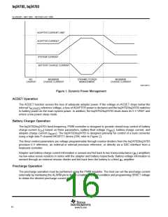
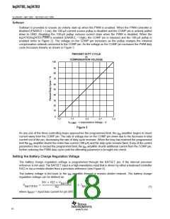
PWM Operation
The three open collector g amplifiers are tied to the COMP pin (refer to Figure 2), which is internally biased
m
up by a 100-µA constant current source. The voltage on the COMP pin is the control voltage (V ) for the PWM
C
comparator. The PWM comparator compares V to the sawtooth ramp of the internally fixed 300-kHz oscillator
C
to provide duty cycle information for the PWM drive. The PWM drive is level-shifted to provide adequate gate
voltage levels for the external P-channel MOSFET. Refer to PWM selector switch gate drive section for gate
drive voltage levels.
Q1
SW
I
+
SW
V
ADPT
V
D1
BAT
ENABLE
CLK
LATCH OUT
S
Q
VCC
OSC
5 V
PWM
DRIVE
RAMP
LEVEL
SHIFT
R
Q
21
PWM
PWM COMPARATOR
FROM ENABLE LOGIC
VHSP
µ
A
100
COMP
10
+
13
BATP
+
BATTERY
VOLTAGE
Z
COMP
ENABLE
1.25 V
BATTERY CHARGE
CURRENT
ADP CURRENT
gm
AMPLIFIERS
UDG−00114
Figure 2. PWM Controller Block Diagram
17
www.ti.com

 TI [ TEXAS INSTRUMENTS ]