ꢀ ꢁꢂ ꢃ ꢄ ꢅ ꢂ ꢆ ꢀꢁ ꢂꢃ ꢄꢅ ꢇ
SLUS553D − MAY 2003 − REVISED JULY 2005
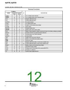
Pin Assignments
ACDET: AC or adapter power detection. This input pin is used to determine the presence of the ac adapter.
When the voltage level on the ACDET pin is less than V , the bq24702/bq24703 is in sleep mode, the
ACPRES
PWM control is disabled, the BATDRV is driven low, and the ACDRV is driven high. This feature can be used
to automatically select battery as the system power source.
ACDRV: AC or adapter power source select output. This pin drives an external P-channel MOSFET used to
switch to the ac wall-adapter as the system power source. When the ACSEL pin is high while the voltage on
the ACDET pin is greater than V
when the ACDET is less than V
, the output ACDRVpin is driven low (V
). This pin is driven high (V
)
ACPRES
HSP
CC
.
ACPRES
ACN, ACP: Negative and positive differential inputs, respectively for ac-to-dc adapter current sense resistor.
ACPRES: This open-drain output pin is used to indicate the presence of ac power. A logic high indicates there
is a valid ac input. A low indicates the loss of ac power. ACPRES is high when the voltage level on the ACDET
pin is greater than V
.
ACPRES
ACSEL: AC adapter power select. This input selects either the ac adapter or the battery as the power source.
A logic high selects ac power, while a logic low selects the battery.
ACSET: Adapter current programming voltage. This input sets the system current level at which dynamic power
management occurs. Adapter currents above this programmed level activate the dynamic power management
and proportionally reduce the available power to the battery.
ALARM: Depleted battery alarm output. This open-drain pin indicates that a depleted battery condition exists.
A pullup on ALARM goes high when the voltage on the BATDEP pin is below V
ALARM output also activates when the selector inputs do not match the selector state.
. On the bq24702, the
ACPRES
BATDEP: Depleted battery level. A voltage divider network from the battery to BATDEP pin is used to set the
battery voltage level at which depletion is indicated by the ALARM pin. See ALARM pin for more details. A
battery depletion is detected when BATDEP is less than V
. A no-battery condition is detected when the
ACPRES
battery voltage is < 80% of the depleted threshold. In a no-battery condition, the bq24702 automatically selects
ac as the input source. If ENABLE = 1, the PWM remains enabled.
BATDRV: Battery power source select output. This pin drives an external P-channel MOSFET used to switch
the battery as the system’s power source. When the voltage level on the ACDET pin is less than V
, the
ACPRES
output of the BATDRV pin is driven low, GND. This pin is driven high (V ) when ACSEL is high and ACDET
CC
> V
.
ACPRES
BATP: Battery charge regulation voltage measurement input to the battery-voltage g amplifier. The voltage
m
on this pin is typically derived from a voltage divider network connected across the battery. In a voltage loop,
BATP is regulated to the V precision reference of the battery voltage g amplifier.
FB
m
BATSET: An external override to an internal precision reference. When BATSET is > 0.25 V, the voltage level
on the BATSET pin sets the voltage charge level. When BATSET ≤ 0.25 V, an internal V reference is
FB
connected to the inverting input of the battery error amplifier. To ensure proper battery voltage regulation with
BATSET, BATSET must be > 1.0 V. Simply ground BATSET to use the internal reference.
COMP: The inverting input to the PWM comparator and output of the g amplifiers. A type II compensation
m
network between COMP and GND is recommended.
ENABLE: Charge enable. A high on this input pin allows PWM control operation to enable charging while a low
on this pin disables and forces the PWM output to a high state. Battery charging is initiated by asserting a logic
1 on the ENABLE pin.
GND: Supply return and ground reference
IBAT: Battery current differential amplifier output. The output of this pin produces a voltage proportional to the
battery charge current. This voltage is suitable for driving an ADC input.
13
www.ti.com

 TI [ TEXAS INSTRUMENTS ]