bq24296
bq24297
www.ti.com
SLUSBP6A –SEPTEMBER 2013–REVISED OCTOBER 2013
HIZ State wth 100mA USB Host
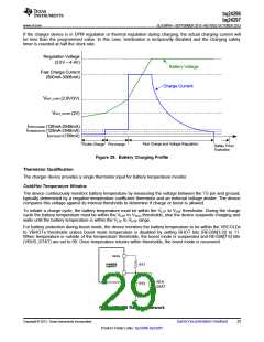
In battery charging spec, the good battery threshold is the minimum charge level of a battery to power up the
portable device successfully. When the input source is 100mA USB host, and the battery is above bat-good
threshold (VBATGD), the device follows battery charging spec and enters high impedance state (HIZ). In HIZ state,
the device is in the lowest quiescent state with REGN LDO and the bias circuits off. The charger device sets
REG00[7] to 1, and the VBUS current during HIZ state will be less than 30µA. The system is supplied by the
battery.
Once the charger device enters HIZ state in host mode, it stays in HIZ until the host writes REG00[7]=0. When
the processor host wakes up, it is recommended to first check if the charger is in HIZ state.
In default mode, the charger IC will reset REG00[7] back to 0 when input source is removed. When another
source plugs in, the charger IC will run detection again, and update the input current limit.
Force Input Current Limit Detection
While adapter is plugged-in, the host can force the charger device to run input current limit detection by setting
REG07[7]=1 or when watchdog timeout. During the forced detection, the input current limit is set to 100mA. After
the detection is completed, REG07[7] will return to 0 by itself and new input current limit is set based on D+/D-
(bq24297) or PSEL/OTG (bq24296).
Converter Power-Up
After the input current limit is set, the converter is enabled and the HSFET and LSFET start switching. If battery
charging is disabled, BATFET turns off. Otherwise, BATFET stays on to charge the battery.
The device provides soft-start when ramp up the system rail. When the system rail is below 2.2V, the input
current limit is forced to 100mA. After the system rises above 2.2V, the charger device sets the input current limit
set by the lower value between register and ILIM pin.
As a battery charger, the charger deploys a 1.5MHz step-down switching regulator. The fixed frequency oscillator
keeps tight control of the switching frequency under all conditions of input voltage, battery voltage, charge current
and temperature, simplifying output filter design.
A type III compensation network allows using ceramic capacitors at the output of the converter. An internal saw-
tooth ramp is compared to the internal error control signal to vary the duty cycle of the converter. The ramp
height is proportional to the PMID voltage to cancel out any loop gain variation due to a change in input voltage.
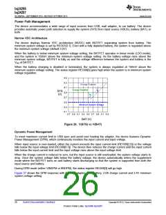
In order to improve light-load efficiency, the device switches to PFM control at light load when battery is below
minimum system voltage setting or charging is disabled. During the PFM operation, the switching duty cycle is
set by the ratio of SYS and VBUS.
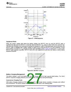
Boost Mode Operation from Battery
The device supports boost converter operation to deliver power from the battery to other portable devices
through USB port. The boost mode output current rating meets the USB On-The-Go 1A output requirement. The
maximum output current is 1.5A. The boost operation can be enabled if the following conditions are valid:
1. BAT above BATLOWV threshold (VBATLOWV set by REG04[1])
2. VBUS less than VBAT + VSLEEP (in sleep mode)
3. Boost mode operation is enabled (OTG pin HIGH and REG01[5:4]=10)
4. Thermistor Temperature is within boost mode temperature monitor threshold unless BHOT[1:0] is set to 11
(REG06[1:0]) to disable this monitor function
5. After 30ms delay from boost mode enable
In boost mode, the device employs a 1.5MHz step-up switching regulator. Similar to buck operation, the device
switches from PWM operation to PFM operation at light load to improve efficiency.
During boost mode, the status register REG08[7:6] is set to 11, the VBUS output is 5V and the output current
can reach up to 1A or 1.5A, selected via I2C (REG01[0]). In addition, the device provides adjustable boost
voltage from 4.55V to 5.5V by changing BOOSTV bits in REG06[7:4]
Any fault during boost operation, including VBUS over-voltage or over-current, sets the fault register REG09[6] to
1 and an INT is asserted.
Copyright © 2013, Texas Instruments Incorporated
Submit Documentation Feedback
25
Product Folder Links: bq24296 bq24297

 TI [ TEXAS INSTRUMENTS ]