bq24296
bq24297
SLUSBP6A –SEPTEMBER 2013–REVISED OCTOBER 2013
www.ti.com
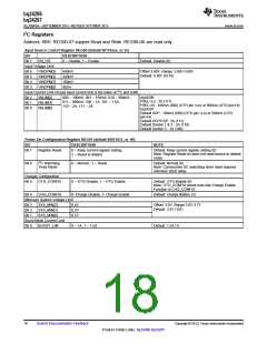
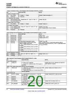
Charge Termination/Timer Control Register REG05 (default 10011010, or 0x9A)
BIT
DESCRIPTION
NOTE
Charging Termination Enable
Bit 7
Bit 6
EN_TERM
Reserved
0 – Disable, 1 – Enable
0 - Reserved
Default: Enable termination (1)
I2C Watchdog Timer Setting
Bit 5
Bit 4
WATCHDOG[1] 00 – Disable timer, 01 – 40s, 10 – 80s, 11 –
Default: 40s (01)
160s
WATCHDOG[0]
Charging Safety Timer Enable
Bit 3 EN_TIMER 0 – Disable, 1 – Enable
Fast Charge Timer Setting
Default: Enable (1)
Bit 2
Bit 1
Bit 0
CHG_TIMER[1] 00 – 5 hrs, 01 – 8 hrs, 10 – 12 hrs, 11 – 20
Default: 12 hrs (10)
(See Charging Safety Timer for details)
hrs
CHG_TIMER[0]
Reserved
0 - Reserved
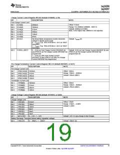
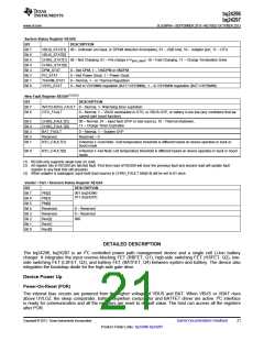
Boost Voltage/Thermal Regulation Control Register REG06 (default 01110011, or 0x73)
BIT
DESCRIPTION
512mV
NOTE
Bit 7
Bit 6
Bit 5
Bit 4
Bit 3
Bit 2
BOOSTV[3]
BOOSTV[2]
BOOSTV[1]
BOOSTV[0]
BHOT[1]
Offset: 4.55V
Range: 4.55V – 5.51V
Default:4.998V(0111)
256mV
128mV
64mV
Set Boost Mode temperature monitor
threshold voltage to disable boost mode
Voltage to disable boost mode
Default: Vbhot1 (00)
Note: For BHOT[1:0]=11, boost mode operates without
temperature monitor and the NTC_FAULT is generated based
BHOT[0]
00 – Vbhot1 (33% of REGN or 55◦C w/ 103AT on Vbhot1 threshold
thermistor)
01 – Vbhot0 (36% of REGN or 60◦C w/ 103AT
thermistor)
10 – Vbhot2 (30% of REGN or 65◦C w/ 103AT
thermistor)
11 – Disable boost mode thermal protection.
Thermal Regulation Threshold
Bit 1
Bit 0
TREG[1]
TREG[0]
00 – 60°C, 01 – 80°C, 10 – 100°C, 11 –
120°C
Default: 120°C (11)
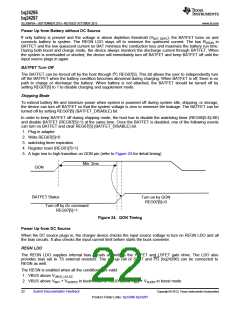
Misc Operation Control Register REG07 (default 01001011, or 4B)
BIT
DESCRIPTION
NOTE
Force DPDM detection
Bit 7
DPDM_EN
0 – Not in D+/D– detection;
1 – Force D+/D– detection when VBUS power is
presence
Default: Not in D+/D– detection (0), Back to 0
after detection complete
Safety Timer Setting during Input DPM and Thermal Regulation
Bit 6
TMR2X_EN
0 – Safety timer not slowed by 2X during input DPM Default: Safety timer slowed by 2X (1)
or thermal regulation,
1 – Safety timer slowed by 2X during input DPM or
thermal regulation
Force BATFET Off
Bit 5
BATFET_Disable
0 – Allow BATFET (Q4) turn on, 1 – Turn off
BATFET (Q4)
Default: Allow BATFET (Q4) turn on(0)
Bit 4
Bit 3
Bit 2
Bit 1
Reserved
0 - Reserved
1 - Reserved
0 - Reserved
Reserved
Reserved
INT_MASK[1]
0 – No INT during CHRG_FAULT, 1 – INT on
CHRG_FAULT
Default: INT on CHRG_FAULT (1)
Default: INT on BAT_FAULT (1)
Bit 0
INT_MASK[0]
0 – No INT during BAT_FAULT, 1 – INT on
BAT_FAULT
20
Submit Documentation Feedback
Copyright © 2013, Texas Instruments Incorporated
Product Folder Links: bq24296 bq24297

 TI [ TEXAS INSTRUMENTS ]