bq24296
bq24297
SLUSBP6A –SEPTEMBER 2013–REVISED OCTOBER 2013
www.ti.com
I2C Registers
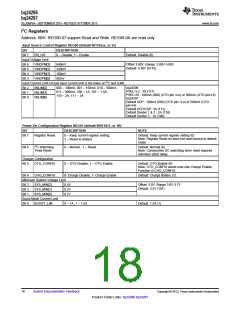
Address: 6BH. REG00-07 support Read and Write. REG08-0A are read only.
Input Source Control Register REG00 (default 00110xxx, or 3x)
BIT
DESCRIPTION
Bit 7
EN_HIZ
0 – Disable, 1 – Enable
Default: Disable (0)
Input Voltage Limit
Bit 6
Bit 5
Bit 4
Bit 3
VINDPM[3]
VINDPM[2]
VINDPM[1]
VINDPM[0]
640mV
320mV
160mV
80mV
Offset 3.88V, Range: 3.88V-5.08V
Default: 4.36V (0110)
Input Current Limit (Actual input current limit is the lower of I2C and ILIM)
Bit 2
Bit 1
Bit 0
IINLIM[2]
IINLIM[1]
IINLIM[0]
000 – 100mA, 001 – 150mA, 010 – 500mA,
011 – 900mA, 100 – 1A, 101 – 1.5A,
110 – 2A, 111 – 3A
bq24296
PSEL=Lo : 3A (111)
PSEL=Hi : 100mA (000) (OTG pin =Lo) or 500mA (OTG pin=Hi)
bq24297
Default SDP : 100mA (000) (OTG pin =Lo) or 500mA (OTG
pin=Hi)
Default DCP/CDP: 3A (111)
Default Divider 1 & 2 : 2A (110)
Default Divider 3 : 1A (100)
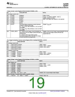
Power-On Configuration Register REG01 (default 00011011, or 1B)
BIT
DESCRIPTION
NOTE
Bit 7
Register Reset
0 – Keep current register setting,
1 – Reset to default
Default: Keep current register setting (0)
Note: Register Reset bit does not reset device to default
mode
Bit 6
I2C Watchdog
Timer Reset
0 – Normal ; 1 – Reset
Default: Normal (0)
Note: Consecutive I2C watchdog timer reset requires
minimum 20uS delay
Charger Configuration
Bit 5
OTG_CONFIG
0 – OTG Disable; 1 – OTG Enable
0- Charge Disable; 1- Charge Enable
Default: OTG disable (0)
Note: OTG_CONFIG would over-ride Charge Enable
Function in CHG_CONFIG
Bit 4
CHG_CONFIG
Default: Charge Battery (1)
Minimum System Voltage Limit
Bit 3
Bit 2
Bit 1
SYS_MIN[2]
SYS_MIN[1]
SYS_MIN[0]
0.4V
0.2V
0.1V
Offset: 3.0V, Range 3.0V-3.7V
Default: 3.5V (101)
Boost Mode Current Limit
Bit 0 BOOST_LIM
0 – 1A, 1 – 1.5A
Default: 1.5A (1)
18
Submit Documentation Feedback
Copyright © 2013, Texas Instruments Incorporated
Product Folder Links: bq24296 bq24297

 TI [ TEXAS INSTRUMENTS ]