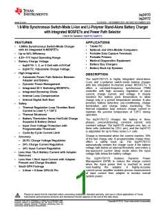
bq24170
bq24172
www.ti.com
SLUSAD2A –NOVEMBER 2010–REVISED NOVEMBER 2010
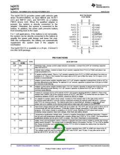
PIN FUNCTIONS (continued)
PIN
TYPE
DESCRIPTION
NO.
NAME
ISET
13
I
Fast charge current set point. Use a voltage divider from VREF to ISET to AGND to set the fast charge
current:
V
ISET
ICHG
=
20´RSR
The pre-charge and termination current is internally as one tenth of the charge current. The charger is
disabled when ISET pin voltage is below 40mV and enabled when ISET pin voltage is above 120mV.
14
CELL
(bq24170)
I
Cell selection pin. Set CELL pin LOW for 1-cell, Float for 2-cell (0.8V-1.8V), and HIGH for 3-cell with a
fixed 4.2V per cell.
FB
(bq24172)
Charge voltage analog feedback adjustment. Connect the output of a resistor divider powered from the
battery terminals to VFB to AGND. Output voltage is regulated to 2.1V on FB pin during constant-voltage
mode.
15
16
17
SRN
I
I/P
I
Charge current sense resistor negative input. A 0.1-mF ceramic capacitor is placed from SRN to SRP to
provide differential-mode filtering. A 0.1-mF ceramic capacitor is placed from SRN pin to AGND for
common-mode filtering.
SRP
Charge current sense resistor, positive input. A 0.1-mF ceramic capacitor is placed from SRN to SRP to
provide differential-mode filtering. A 0.1-mF ceramic capacitor is placed from SRP pin to AGND for
common-mode filtering.
ACSET
Input current set point. Use a voltage divider from VREF to ACSET to AGND to set this value:
VACSET
IDPM
=
20´RAC
18
19
OVPSET
BATDRV
I
Valid input voltage set point. Use a voltage divider from input to OVPSET to AGND to set this voltage.
The voltage above internal 1.6V reference indicates input over-voltage, and the voltage below internal
0.5V reference indicates input under-voltage. In either condition, charge terminates, and input NMOS pair
ACFET/RBFET turn off. LED driven by STAT pin keeps blinking, reporting fault condition.
O
Battery discharge MOSFET gate driver output. Connect to 1kohm resistor to the gate of the BATFET
P-channel power MOSFET. Connect the source of the BATFET to the system load voltage node. Connect
the drain of the BATFET to the battery pack positive node. The internal gate drive is asymmetrical to
allow a quick turn-off and slower turn-on, in addition to the internal break-before-make logic with respect
to ACDRV. There is an internal pull-down resistor of 50k on BATDRV to ground.
20
REGN
P
PWM low side driver positive 6V supply output. Connect a 1-mF ceramic capacitor from REGN to PGND
pin, close to the IC. Generate high-side driver bootstrap voltage by integrated diode from REGN to BTST.
21
BTST
P
P
PWM high side driver positive supply. Connect the 0.047-µF bootstrap capacitor from SW to BTST.
22,23
PGND
Power ground. Ground connection for high-current power converter node. On PCB layout, connect
directly to ground connection of input and output capacitors of the charger. Only connect to AGND
through the Thermal Pad underneath the IC.
Thermal AGND
Pad
P
Exposed pad beneath the IC. Always solder Thermal Pad to the board, and have vias on the Thermal
Pad plane star-connecting to AGND and ground plane for high-current power converter. It dissipates the
heat from the IC.
Copyright © 2010, Texas Instruments Incorporated
Submit Documentation Feedback
3
Product Folder Link(s): bq24170 bq24172

 TI [ TEXAS INSTRUMENTS ]