bq24170
bq24172
SLUSAD2A –NOVEMBER 2010–REVISED NOVEMBER 2010
www.ti.com
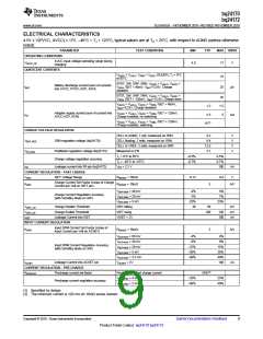
RGY PACKAGE
(TOP VIEW)
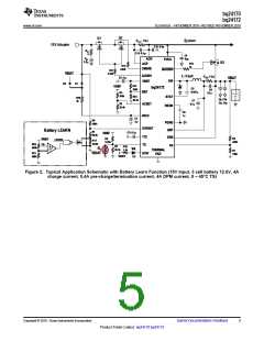
The bq24170/172 provides power path selector gate
driver ACDRV/CMSRC on input NMOS pair ACFET
(Q1) and RBFET (Q2), and BATDRV on a battery
PMOS device (Q3). When the qualified adapter is
present, the system is directly connected to the
adapter. Otherwise, the system is connected to the
battery. In addition, the power path prevents battery
from boosting back to the input.
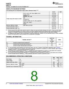
1
24
2
3
23
22
21
20
19
18
17
16
15
14
PVCC
PVCC
AVCC
ACN
PGND
PGND
BTST
REGN
4
5
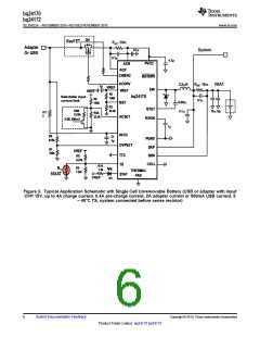
For 1 cell applications, if the battery is not removable,
the system can be directly connected to the battery to
simplify the power path design and lower the cost.
With this configuration, the battery can automatically
supplement the system load if the adapter is
overloaded.
6
ACP
BATDRV
OVPSET
ACSET
SRP
7
CMSRC
ACDRV
STAT
TS
AGND
8
9
10
11
SRN
TTC
CELL/FB
12
13
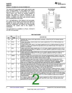
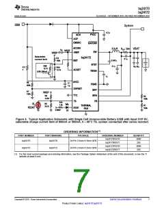
The bq24170/172 is available in a 24-pin, 3.5mmx5.5
mm thin QFN package.
PIN FUNCTIONS
PIN
TYPE
DESCRIPTION
NO.
NAME
SW
1,24
P
Switching node, charge current output inductor connection. Connect the 0.047-µF bootstrap capacitor
from SW to BTST.
2,3
4
PVCC
AVCC
P
P
Charger input voltage. Connect at least 10-µF ceramic capacitor from PVCC to PGND and place it as
close as possible to IC.
IC power positive supply. Place a 1-µF ceramic capacitor from AVCC to AGND and place it as close as
possible to IC. Place a 10-Ω resistor from input side to AVCC pin to filter the noise. For 5V input, a 5-Ω
resistor is recommended.
5
6
7
8
ACN
I
Adapter current sense resistor negative input. A 0.1-µF ceramic capacitor is placed from ACN to ACP to
provide differential-mode filtering. An optional 0.1-µF ceramic capacitor is placed from ACN pin to AGND
for common-mode filtering.
ACP
P/I
O
Adapter current sense resistor positive input. A 0.1-µF ceramic capacitor is placed from ACN to ACP to
provide differential-mode filtering. A 0.1-µF ceramic capacitor is placed from ACP pin to AGND for
common-mode filtering.
CMSRC
ACDRV
Connect to common source of N-channel ACFET and reverse blocking MOSFET (RBFET). Place 4-kΩ
resistor from CMSRC pin to the common source of ACFET and RBFET to control the turn-on speed. The
resistance between ACDRV and CMSRC should be 500-kΩ or bigger.
O
AC adapter to system switch driver output. Connect to 4-kΩ resistor then to the gate of the ACFET
N-channel power MOSFET and the reverse conduction blocking N-channel power MOSFET. Connect
both FETs as common-source. The internal gate drive is asymmetrical, allowing a quick turn-off and
slower turn-on in addition to the internal break-before-make logic with respect to the BATDRV.
9
STAT
O
Open-drain charge status pin with 10-kΩ pull up to power rail. The STAT pin can be used to drive LED or
communicate with the host processor. It indicates various charger operations: LOW when charge in
progress. HIGH when charge is complete or in SLEEP mode. Blinking at 0.5Hz when fault occurs,
including charge suspend, input over-voltage, timer fault and battery absent.
10
11
TS
I
I
Temperature qualification voltage input. Connect a negative temperature coefficient thermistor. Program
the hot and cold temperature window with a resistor divider from VREF to TS to AGND. The temperature
qualification window can be set to 5-40°C or wider. The 103AT thermistor is recommended.
TTC
Safety Timer and termination control. Connect a capacitor from this node to AGND to set the fast charge
safety timer(5.6min/nF). Pre-charge timer is internally fixed to 30 minutes. Pull the TTC to LOW to disable
the charge termination and safety timer. Pull the TTC to HIGH to disable the safety timer but allow the
charge termination.
12
VREF
P
3.3V reference voltage output. Place a 1-mF ceramic capacitor from VREF to AGND pin close to the IC.
This voltage could be used for programming ISET and ACSET and TS pins. It may also serve as the
pull-up rail of STAT pin and CELL pin.
2
Submit Documentation Feedback
Copyright © 2010, Texas Instruments Incorporated
Product Folder Link(s): bq24170 bq24172

 TI [ TEXAS INSTRUMENTS ]