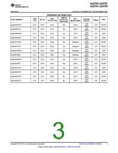
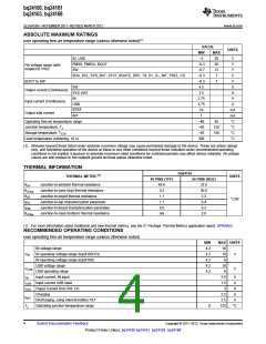
bq24160, bq24161
bq24163, bq24168
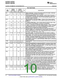
SLUSAO0A –NOVEMBER 2011–REVISED MARCH 2012
www.ti.com
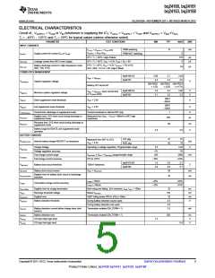
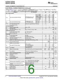
ELECTRICAL CHARACTERISTICS (Continued)
Circuit of Figure 23, VSUPPLY = VUSB or VIN (whichever is supplying the IC), VUVLO < VSUPPLY < VOVP and VSUPPLY > VBAT+VSLP
TJ = -40°C – 125°C and TJ = 25ºC for typical values (unless otherwise noted)
,
PARAMETER
TEST CONDITIONS
MIN
TYP
MAX
UNIT
INPUT CURRENT LIMITING
IUSBLIM = USB100
90
450
135
800
700
1250
1.35
2.3
95
475
100
500
150
900
800
1500
1.65
2.8
IUSBLIM = USB500
IUSBLIM = USB150
IUSBLIM = USB900
IUSBLIM = USB800
IUSBLIM = 1.5A
142.5
850
USB charge mode, VUSB = 5V,
DC Current pulled from SW
IIN_USB
Input current limit threshold (USB input)
Input current limit threshold (IN input)
mA
750
1400
1.5
IN charge mode, VIN = 5V,
DC Current pulled from SW
IINLIM = 1.5A
IIN_IN
A
V
IINLIM = 2.5A
2.5
Charge mode, programmable via I2C, both inputs
VIN_DPM
Input based DPM threshold range
VIN_DPM threshold accuracy
4.2
4.76
–2
+2%
5.45
450
VDRV BIAS REGULATOR
VDRV
Internal bias regulator voltage
VSUPPLY > 5.45V
5
5.2
V
IDRV
DRV output current
10
mA
mV
VDO_DRV
DRV Dropout voltage (VSUPPLY – VDRV
)
ISUPPLY = 1A, VSUPPLY = 5V, IDRV = 10mA
STATUS OUTPUT (STAT, INT)
VOL
Low-level output saturation voltage
IO = 10mA, sink current
VSTAT = VINT = 5V
0.4
1
V
IIH
High-level leakage current
µA
PROTECTION
VUVLO
IC active threshold voltage
IC active hysteresis
VIN rising
3.6
120
0
3.8
150
40
4
V
VUVLO_HYS
VSLP
VIN falling from above VUVLO
2.0V ≤VBAT ≤VBATREG, VIN falling
2.0V ≤VBAT ≤VBATREG
mV
mV
mV
ms
Sleep-mode entry threshold, VSUPPLY-VBAT
Sleep-mode exit hysteresis
100
175
VSLP_EXIT
40
100
30
Deglitch time for supply rising above VSLP+VSLP_EXIT
Rising voltage, 2mV over drive, tRISE = 100ns
VIN_DPM
– 80 mV
VBAD_SOURCE Bad source detection threshold
Deglitch on bad source detection
V
32
6.5
ms
USB, VUSB Rising
6.3
10.3
6.3
6.7
10.7
6.7
VOVP
Input supply OVP threshold voltage
IN, VIN Rising (bq24160/1/3)
IN, VIN Rising (bq24168)
Supply falling from VOVP
10.5
6.5
V
VOVP(HYS)
VBOVP
VOVP hysteresis
100
mV
V
1.025 ×
VBATREG
1.05 ×
VBATREG
1.075 ×
VBATREG
Battery OVP threshold voltage
VBAT threshold over VOREG to turn off charger during charge
Lower limit for VBAT falling from above VBOVP
% of
VBATREG
VBOVP hysteresis
1
VBATUVLO
ILIMIT
Battery undervoltage lockout threshold
Cycle-by-cycle current limit
Thermal trip
VBAT rising, 100mV hysteresis
VSYS shorted
2.5
4.9
165
10
V
A
4.1
5.6
TSHTDWN
°C
Thermal hysteresis
TREG
Thermal regulation threshold
Safety timer accuracy
Charge current begins to cut off
(bq24160/1/3 Only)
120
°C
–20%
20%
PWM
IIN_LIMIT = 500mA, Measured from USB to PMIDU
IIN_LIMIT = 500mA, Measured from IN to PMIDI
Measured from PMIDU to SW
95
45
175
80
Internal top reverse blocking MOSFET on-resistance
mΩ
mΩ
100
65
175
110
115
1.65
Internal top N-channel Switching MOSFET on-
resistance
Measured from PMIDI to SW
Internal bottom N-channel MOSFET on-resistance
Oscillator frequency
Measured from SW to PGND
65
mΩ
fOSC
1.35
0%
1.50
95%
MHz
DMAX
DMIN
Maximum duty cycle
Minimum duty cycle
6
Submit Documentation Feedback
Copyright © 2011–2012, Texas Instruments Incorporated
Product Folder Link(s): bq24160 bq24161 bq24163 bq24168

 TI [ TEXAS INSTRUMENTS ]