bq24160, bq24161
bq24163, bq24168
SLUSAO0A –NOVEMBER 2011–REVISED MARCH 2012
www.ti.com
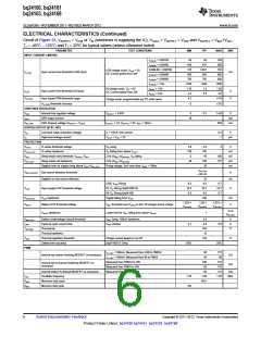
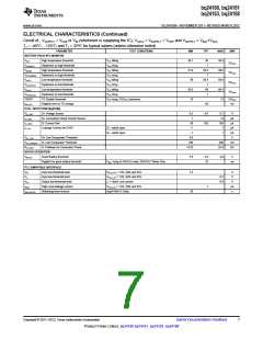
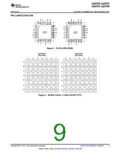
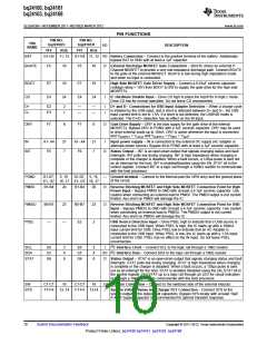
PIN FUNCTIONS
PIN NO.
bq24160/3
PIN NO.
bq24161/8
PIN
NAME
I/O
DESCRIPTION
YFF
RGE
YFF
RGE
BAT
G1-G4
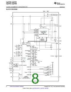
11, 12 G1-G4 11, 12 I/O Battery Connection – Connect to the positive terminal of the battery. Additionally,
bypass BAT to GND with at least a 1μF capacitor.
BGATE
F5
10
F5
10
O
External Discharge MOSFET Gate Connection – BGATE drives an external P-
Channel MOSFET to provide a very low-resistance discharge path. Connect BGATE
to the gate of the external MOSFET. BGATE is low during high impedance mode
and when no input is connected.
BOOT
CD
E7
E4
19
24
E7
E4
19
24
I
I
High Side MOSFET Gate Driver Supply – Connect a 0.01µF ceramic capacitor
(voltage rating > 10V) from BOOT to SW to supply the gate drive for the high side
MOSFETs.
IC Hardware Disable Input – Drive CD high to place the bq2416x in high-z mode.
Drive CD low for normal operation. Do not leave CD unconnected.
D+
D–
E2
E3
2
1
—
—
—
—
I
I
D+ and D– Connections for USB Input Adapter Detection – When a charge cycle
is initiated by the USB input, and a short is detected between D+ and D–, the USB
input current limit is set to 1.5A. If a short is not detected, the USB100 mode is
selected. The D+/D– detection has no effect on the IN input.
DRV
F7
6
F7
6
O
Gate Drive Supply – DRV is the bias supply for the gate drive of the internal
MOSFETs. Bypass DRV to PGND with a 1μF ceramic capacitor. DRV may be used
to drive external loads up to 10mA. DRV is active whenever the input is connected
and VSUPPLY > VUVLO and VSUPPLY > (VBAT + VSLP
)
IN
A1- A4
F6
21
7
A1- A4
F6
21
7
I
Input power supply – IN is connected to the external DC supply (AC adapter or
alternate power source). Bypass IN to PGND with at least a 1μF ceramic capacitor.
INT
O
Status Output – INT is an open-drain output that signals charging status and fault
interrupts. INT pulls low during charging. INT is high impedance when charging is
complete or the charger is disabled. When a fault occurs, a 128μs pulse is sent out
as an interrupt for the host. INT is enabled/disabled using the EN_STAT bit in the
control register. Connect INT to a logic rail through a 100kΩ resistor to communicate
with the host processor.
PGND
PMIDI
D1-D7,
5, 15,
D1-D7, 5, 15,
—
O
Ground terminal – Connect to the thermal pad (for QFN only) and the ground plane
of the circuit.
E1, G7 16, 17 E1, G7 16, 17
B1-B4
B5-B7
—
20
23
—
B1-B4
B5-B7
E2
20
23
2
Reverse Blocking MOSFET and High Side MOSFET Connection Point for High
Power Input – Bypass PMIDI to GND with at least a 4.7μF ceramic capacitor. Use
caution when connecting an external load to PMIDI. The PMIDI output is not current
limited. Any short on PMIDI will damage the IC.
PMIDU
PSEL
O
Reverse Blocking MOSFET and High Side MOSFET Connection Point for USB
Input – Bypass PMIDU to GND with at least a 4.7μF ceramic capacitor. Use caution
when connecting an external load to PMIDU. The PMIDU output is not current
limited. Any short on PMIDU will damage the IC.
USB Source Detection Input – Drive PSEL high to indicate that a USB source is
connected to the USB input. When PSEL is high, the IC starts up with a 100mA
input current limit for USB. Drive PSEL low to indicate that an AC Adapter is
connected to the USB input. When PSEL is low, the IC starts up with a 1.5A input
current limit for USB. PSEL has no effect on the IN input. Do not leave PSEL
unconnected.
SCL
E6
E5
G6
3
4
8
E6
E5
G6
3
4
8
I
I2C Interface Clock – Connect SCL to the logic rail through a 10kΩ resistor.
SDA
STAT
I/O I2C Interface Data – Connect SDA to the logic rail through a 10kΩ resistor.
O
Status Output – STAT is an open-drain output that signals charging status and fault
interrupts. STAT pulls low during charging. STAT is high impedance when charging
is complete or the charger is disabled. When a fault occurs, a 128μs pulse is sent
out as an interrupt for the host. STAT is enabled /disabled using the EN_STAT bit in
the control register. Pull STAT up to a logic rail thruogh an LED for visual indication
or through a 10kΩ resistor to communicate with the host processor.
SW
C1-C7
F1-F4
18
C1-C7
F1-F4
18
O
I
Inductor Connection – Connect to the switched side of the external inductor.
SYS
13, 14
13,14
System Voltage Sense and Charger FET Connection – Connect SYS to the
system output at the output bulk capacitors. Bypass SYS locally with at least 10μF.
A 47μF bypass capacitor is recommended for optimal transient response.
10
Submit Documentation Feedback
Copyright © 2011–2012, Texas Instruments Incorporated
Product Folder Link(s): bq24160 bq24161 bq24163 bq24168

 TI [ TEXAS INSTRUMENTS ]