bq24160, bq24161
bq24163, bq24168
www.ti.com
SLUSAO0A –NOVEMBER 2011–REVISED MARCH 2012
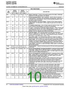
PIN FUNCTIONS (continued)
PIN NO.
bq24160/3
PIN NO.
bq24161/8
PIN
NAME
I/O
DESCRIPTION
YFF
RGE
YFF
RGE
TS
G5
9
G5
9
I
Battery Pack NTC Monitor – Connect TS to the center tap of a resistor divider from
DRV to GND. The NTC is connected from TS to GND. The TS function provides 4
thresholds for JEITA compatibility (160/163/168 only). TS faults are reported by the
I2C interface. See the NTC Monitor section for more details on operation and
selecting the resistor values. Connect TS to DRV to disable the TS function.
USB
A5-A7
—
22
A5-A7
—
22
I
USB Input Power Supply – USB is connected to the external DC supply (AC
adapter or USB port). Bypass USB to PGND with at least a 1μF ceramic capacitor.
Thermal
Pad
Pad
Pad
—
There is an internal electrical connection between the exposed thermal pad and the
PGND pin of the device. The thermal pad must be connected to the same potential
as the PGND pin on the printed circuit board. Do not use the thermal pad as the
primary ground input for the device. PGND pin must be connected to ground at all
times.
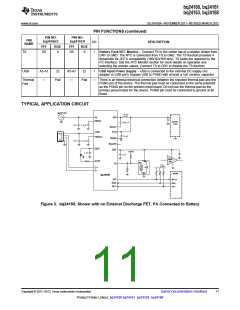
TYPICAL APPLICATION CIRCUIT
ADAPTER
1.5 mH
IN
SW
PMIDI
System
Load
0.01 mF
1 mF
4.7 mF
BOOT
SYS
USB
VBUS
D+
D-
10 mF
PMIDU
PGND
GND
1 mF
4.7 mF
BGATE
DRV
BAT
TS
VDRV
1 mF
1 mF
GSM
PA
PACK+
STAT
TEMP
VSYS
(1.8V)
D+
D-
PACK-
HOST
bq24160
GPIO1
INT
SDA
SCL
SDA
SCL
Figure 3. bq24160, Shown with no External Discharge FET, PA Connected to Battery
Copyright © 2011–2012, Texas Instruments Incorporated
Submit Documentation Feedback
11
Product Folder Link(s): bq24160 bq24161 bq24163 bq24168

 TI [ TEXAS INSTRUMENTS ]