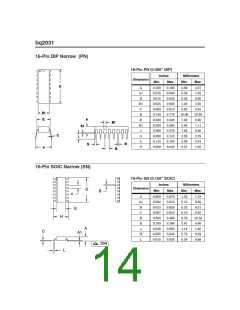
bq2031
Voltage at the SNS pin is determined by the value of re-
sistor RSNS, so nominal regulated current is set by:
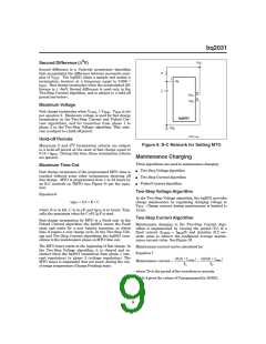
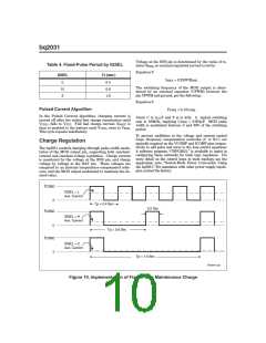
Table 4. Fixed-Pulse Period by IGSEL
Equation 8
IGSEL
TP (sec.)
IMAX = 0.250V/RSNS
L
H
Z
0.4
0.8
1.6
The switching frequency of the MOD output is deter-
mined by an external capacitor (CPWM) between the
pin TPWM and ground, per the following:
Equation 9
Pulsed Current Algorithm
FPWM = 0.1/CPWM
In the Pulsed Current algorithm, charging current is
turned off after the initial fast charge termination until
where C is in µF and F is in kHz.
A
typical switching
rate is 100kHz, implying CPWM = 0.001µF. MOD pulse
width is modulated between 0 and 80% of the switching
period.
VCELL falls to VFLT
. Full fast charge current (IMAX) is
then re-enabled to the battery until VCELL rises to VBLK
This cycle repeats indefinitely.
.
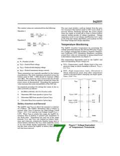
To prevent oscillation in the voltage and current control
loops, frequency compensation networks (C or R-C) are
typically required on the VCOMP and ICOMP pins (respec-
tively) to add poles and zeros to the loop control equations.
A software program, “CNFG2031,” is available to assist in
configuring these networks for buck type regulators. For
more detail on the control loops in buck topology, see the
application note, “Switch-Mode Power Conversion Using
the bq2031.” For assistance with other power supply topolo-
gies, contact the factory.
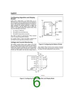
Charge Regulation
The bq2031 controls charging through pulse-width modu-
lation of the MOD output pin, supporting both constant-
current and constant-voltage regulation. Charge current
is monitored by the voltage at the SNS pin, and charge
voltage by voltage at the BAT pin. These voltages are
compared to an internal temperature-compensated refer-
ence, and the MOD output modulated to maintain the de-
sired value.
I
COND
IGSEL = L
Ave. Current
0
T
= 0.4 Sec
P
0.2 Sec
I
COND
IGSEL = H
Ave. Current
0
T
= 0.8 Sec
P
I
COND
IGSEL = Z
Ave. Current
0
T
= 1.6 Sec
P
TD203101.eps
Figure 10. Implementation of Fixed-Pulse Maintenance Charge
10

 TI [ TEXAS INSTRUMENTS ]