AM6548, AM6528, AM6526
ZHCSLA7B –DECEMBER 2019 –REVISED JUNE 2021
www.ti.com.cn
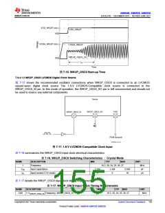
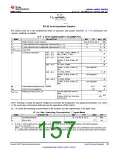
表7-17. WKUP_OSC0 Input Clock Timing Requirements (continued)
NAME
DESCRIPTION
MIN
TYP
MAX
UNIT
CK1
tw(WKUP_OSC0_XI)
Pulse duration, WKUP_OSC0_XI low or high
Period jitter, WKUP_OSC0_XI
0.45 ×
tc(WKUP_OSC0_XI)
0.55 ×
tc(WKUP_OSC0_XI)
ns
tj(WKUP_OSC0_XI)
0.01 ×
ns
tc(WKUP_OSC0_XI)
tR(WKUP_OSC0_XI)
tF(WKUP_OSC0_XI)
tj(WKUP_OSC0_XI)
Rise time, WKUP_OSC0_XI
Fall time, WKUP_OSC0_XI
5
5
ns
ns
Frequency accuracy,
WKUP_OSC0_XI
Ethernet RGMII and RMII
not used
±100
ppm
Ethernet RGMII and RMII
using derived clock
±50
CK0
CK1
CK1
WKUP_OSC0_XI
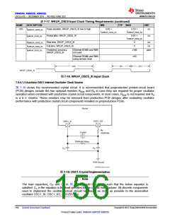
图7-18. WKUP_OSC0_XI Input Clock
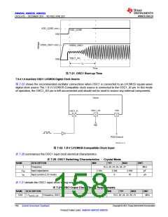
7.9.4.1.3 Auxiliary OSC1 Internal Oscillator Clock Source
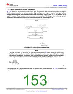
图 7-19 shows the recommended crystal circuit. It is recommended that preproduction printed-circuit board
(PCB) designs include the two optional resistors Rbias and Rd in case they are required for proper oscillator
operation when combined with production crystal circuit components. In most cases, Rbias is not required and Rd
is a 0-Ω resistor. These resistors may be removed from production PCB designs after evaluating oscillator
performance with production crystal circuit components installed on preproduction PCBs.
Device
OSC1_XO
OSC1_XI
Rd
(Optional)
Crystal
(Optional)
Rbias
Cf2
Cf1
PCB Ground
SPRSP08_PCB_CLK_OSC_1
图7-19. OSC1 Crystal Implementation
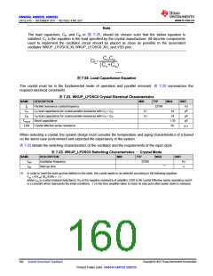
Note
The load capacitors, Cf1 and Cf2 in 图 7-20, should be chosen such that the below equation is
satisfied. CL in the equation is the load specified by the crystal manufacturer. All discrete components
used to implement the oscillator circuit should be placed as close as possible to the associated
oscillator OSC1_XI, OSC1_XO, and VSS pins.
Copyright © 2021 Texas Instruments Incorporated
156 Submit Document Feedback
Product Folder Links: AM6548 AM6528 AM6526

 TI [ TEXAS INSTRUMENTS ]