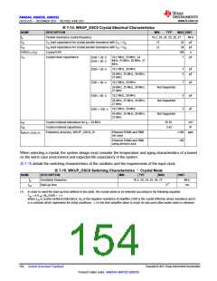
AM6548, AM6528, AM6526
ZHCSLA7B –DECEMBER 2019 –REVISED JUNE 2021
www.ti.com.cn
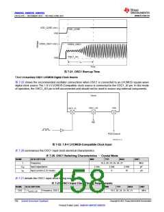
VDD_CORE (min.)
VSS
VDD_CORE
VDDS_OSC1
VDDS_OSC1 (min.)
OSC1_XO
tsX
VSS
Time
图7-21. OSC1 Start-up Time
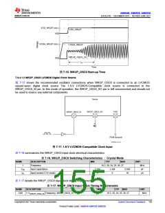
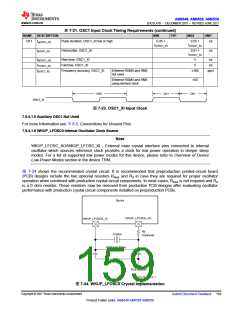
7.9.4.1.4 Auxiliary OSC1 LVCMOS Digital Clock Source
图 7-22 shows the recommended oscillator connections when OSC1 is connected to an LVCMOS square-wave
digital clock source The 1.8-V LVCMOS-Compatible clock source is connected to the OSC1_XI pin. In this mode
of operation, the OSC1_XO pin is left unconnected and should not be used to source any external components.
Device
OSC1_XO
VSS
OSC1_XI
NC
PCB Ground
SPRSP08_CLK_01
图7-22. 1.8-V LVCMOS-Compatible Clock Input
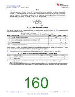
表7-20 summarizes the OSC1 input clock electrical characteristics.
表7-20. OSC1 Switching Characteristics –Crystal Mode
NAME
DESCRIPTION
MIN
TYP
MAX
UNIT
MHz
f
Frequency
19.2, 20, 24, 25, 26, 27
CIN
IIN
Input capacitance
Input current (3.3V mode)
2.184
4
2.384
6
2.584
10
pF
µA
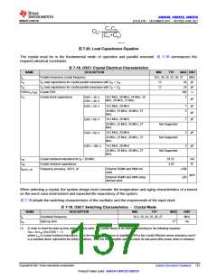
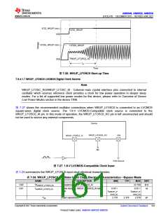
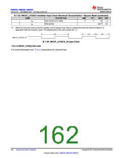
表7-21 details the OSC1 input clock timing requirements.
表7-21. OSC1 Input Clock Timing Requirements
NAME DESCRIPTION
CK0 1 / tc(OSC1_XI)
MIN
TYP
MAX
UNIT
Frequency, OSC1_XI
19.2, 20, 24, 25, 26, 27
MHz
Copyright © 2021 Texas Instruments Incorporated
158 Submit Document Feedback
Product Folder Links: AM6548 AM6528 AM6526

 TI [ TEXAS INSTRUMENTS ]