AM6548, AM6528, AM6526
ZHCSLA7B –DECEMBER 2019 –REVISED JUNE 2021
www.ti.com.cn
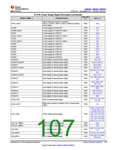
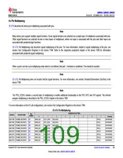
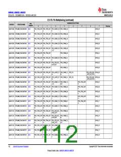
表6-75. Power Supply Signal Description (continued)
PIN TYPE
SIGNAL NAME [1]
VDD_WKUP0(4)
VDD_WKUP1(4)
DESCRIPTION [2]
BALL [4]
[3]
WKUP voltage domain supply
WKUP voltage domain supply
PWR
PWR
V11, W10, W12
M22
A1, A2, A28, AA11,
AA13, AA15, AA17,
AA19, AA23, AA26,
AA7, AB10, AB12,
AB14, AB16, AB18,
AB20, AB22, AD4,
AE10, AE25, AE5,
AF15, AF2, AF20,
AF8, AG1, AG10,
AG28, AG4, AG7,
AH1, AH11, AH2,
AH27, AH28, AH5,
AH8, B12, B15, B20,
B6, B9, D22, E26,
E28, E4, F14, F19,
F22, F25, F27, F3,
G11, G13, G16, G2,
G21, G23, G7, G9,
H1, H10, H12, H14,
H20, H22, H24, H26,
H28, H6, H8, J11,
J13, J15, J18, J21,
J23, J25, J27, J7, J9,
K1, K10, K12, K14,
K17, K19, K22, K23,
K6, K8, L11, L13,
VSS
Ground
GND
L16, L23, L24, L26,
L28, L3, L7, L9, M10,
M15, M17, M20, M8,
N11, N13, N16, N19,
N21, N7, N9, P10,
P12, P14, P16, P18,
P22, P6, P8, R11,
R13, R15, R17, R19,
R21, R7, R9, T10,
T12, T14, T16, T18,
T22, T26, T8, U11,
U13, U15, U17, U19,
U21, U3, U7, U9,
V10, V12, V14, V18,
V20, V22, V6, W11,
W13, W15, W17,
W19, W21, W23, W7,
W9, Y12, Y14, Y16,
Y18, Y22, Y6, Y8
(1) This pin must always be connected via a 1-µF capacitor to VSS.
(2) The net connecting CAP_VDDA_1P8_SDIO and VDDA_1P8_SDIO to VDDS6 or VDDS7 must be connected to a 3.3-uF decoupling
capacitor. VDDA_1P8_SDIO, CAP_VDDA_1P8_SDIO, CAP_VDDSHV_SDIO, and VDDA_3P3_SDIO must be connected to VSS,
when SDIO_LDO is not used with either MMC0 or MMC1.
(3) When CAP_VDDSHV_SDIO is connected to VDDSHV6 or VDDSHV7, the entire net which connects these pins should not exceed 6-
uF of decoupling capacitance. VDDA_1P8_SDIO, CAP_VDDA_1P8_SDIO, CAP_VDDSHV_SDIO, and VDDA_3P3_SDIO must be
connected to VSS, when SDIO_LDO is not used with either MMC0 or MMC1.
(4) These power rails should be connected together on the board level.
(5) VDDA_POR_WKUP is preferred to be connected to CAP_VDDA_1P8_IOLDO_WKUP when using internal POR feature.
(6) The VDDA_VSYS_MON pin provides a way to monitor the system power supply and is not fail-safe, unless implemented with the
appropriate resistor voltage divider source. For more information, see 节9.2.5, System Power Supply Monitor Design Guidelines.
Copyright © 2021 Texas Instruments Incorporated
108 Submit Document Feedback
Product Folder Links: AM6548 AM6528 AM6526

 TI [ TEXAS INSTRUMENTS ]