AM6548, AM6528, AM6526
ZHCSLA7B –DECEMBER 2019 –REVISED JUNE 2021
www.ti.com.cn
6.4 Pin Multiplexing
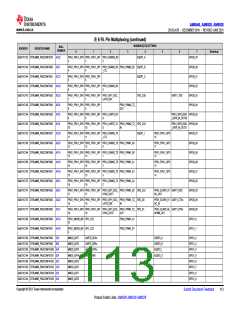
表6-76 describes the device pin multiplexing associated with pins.
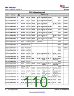
Note
Many device pins support multiple signal functions. Some signal functions are selected via a single layer of multiplexers associated with pins.
Other signal functions are selected via two or more layers of multiplexers, where one layer is associated with the pins and other layers are
associated with peripheral logic functions.
表 6-76, Pin Multiplexing only describes signal multiplexing at the pins. For more information, related to signal multiplexing at the pins, see
section Pad Configuration Registers in the device TRM. Refer to the respective peripheral chapter in the device TRM for information
associated with peripheral signal multiplexing.
Note
When a pad is set into a pin multiplexing mode which is not defined, that pad’s behavior is undefined. This should be avoided.
Note
表 6-76, Pin Multiplexing does not include SerDes signal functions. For more information, see section Serializer/Deserializer (SerDes) in the
device TRM.
Note
The PRU_ICSSG contains a second layer of multiplexing to enable additional functionality on the PRU GPO and GPI signals. This internal
wrapper multiplexing is described in the PRU_ICSSG chapter in the device TRM.
For more information on the I/O cell configurations, see section Pad Configuration Registers in the device TRM.
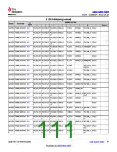
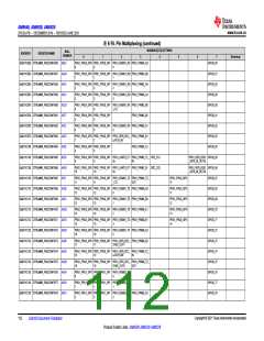
表6-76. Pin Multiplexing
MUXMODE[7:0] SETTINGS
BALL
ADDRESS
REGISTER NAME
NUMBER
M27
0
1
2
3
4
5
6
7
Bootstrap
BOOTMODE00
BOOTMODE01
BOOTMODE02
BOOTMODE03
BOOTMODE04
BOOTMODE05
BOOTMODE06
BOOTMODE07
0x0011C000 CTRLMMR_PADCONFIG0
0x0011C004 CTRLMMR_PADCONFIG1
0x0011C008 CTRLMMR_PADCONFIG2
0x0011C00C CTRLMMR_PADCONFIG3
0x0011C010 CTRLMMR_PADCONFIG4
0x0011C014 CTRLMMR_PADCONFIG5
0x0011C018 CTRLMMR_PADCONFIG6
0x0011C01C CTRLMMR_PADCONFIG7
GPMC0_AD0
GPMC0_AD1
GPMC0_AD2
GPMC0_AD3
GPMC0_AD4
GPMC0_AD5
GPMC0_AD6
GPMC0_AD7
VOUT1_DATA0
VOUT1_DATA1
VOUT1_DATA2
VOUT1_DATA3
VOUT1_DATA4
VOUT1_DATA5
VOUT1_DATA6
VOUT1_DATA7
VIN0_DATA12
VIN0_DATA13
VIN0_DATA14
VIN0_DATA15
GPIO0_0
M23
M28
M24
N24
N27
N28
M25
GPIO0_1
GPIO0_2
GPIO0_3
GPIO0_4
GPIO0_5
GPIO0_6
GPIO0_7
Copyright © 2021 Texas Instruments Incorporated
Submit Document Feedback
109
Product Folder Links: AM6548 AM6528 AM6526

 TI [ TEXAS INSTRUMENTS ]