AM3359, AM3358, AM3357
AM3356, AM3354, AM3352
www.ti.com
SPRS717F –OCTOBER 2011–REVISED APRIL 2013
from an external power supply.
(5) During functional operation, this pin is a no connect.
(6) Not availabe on the ZCE package.
(7) This terminal is connected to a fail-safe IO and does not have a dependence on any IO supply voltage.
(8) This parameter applies to all IO terminals which are not fail-safe and the requirement applies to all values of IO supply voltage. For
example, if the voltage applied to a specific IO supply is 0 volts the valid input voltage range for any IO powered by that supply will be
‑0.5 to +0.3 volts. Special attention should be applied anytime peripheral devices are not powered from the same power sources used to
power the respective IO supply. It is important the attached peripheral never sources a voltage outside the valid input voltage range,
including power supply ramp-up and ramp-down sequences.
(9) This terminal is connected to analog circuits in the respective USB PHY. The circuit sources a known current while measuring the
voltage to determine if the terminal is connected to VSSA_USB with a resistance less than 10 Ω or greater than 100 kΩ. The terminal
should be connected to ground for USB host operation or open-circuit for USB peripheral operation, and should never be connected to
any external voltage source.
(10) For tape and reel the storage temperature range is [-10°C; +50°C] with a maximum relative humidity of 70%. It is recommended
returning to ambient room temperature before usage.
(11) Based on JEDEC JESD22-A114E [Electrostatic Discharge (ESD) Sensitivity Testing Human Body Model (HBM)].
(12) Based on JEDEC JESD22-C101C (Field-Induced Charged-Device Model Test Method for Electrostatic-Discharge-Withstand
Thresholds of Microelectronic Components).
(13) Based on JEDEC JESD78D [IC Latch-Up Test].
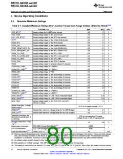
Fail-safe IO terminals are designed such they do not have dependencies on the respective IO power supply
voltage. This allows external voltage sources to be connected to these IO terminals when the respective IO
power supplies are turned off. The USB0_VBUS and USB1_VBUS are the only fail-safe IO terminals. All other IO
terminals are not fail-safe and the voltage applied to them should be limited to the value defined by the Steady
State Max. Voltage at all IO pins parameter in Table 3-1.
Copyright © 2011–2013, Texas Instruments Incorporated
Device Operating Conditions
81
Submit Documentation Feedback
Product Folder Links: AM3359 AM3358 AM3357 AM3356 AM3354 AM3352

 TI [ TEXAS INSTRUMENTS ]