AM3359, AM3358, AM3357
AM3356, AM3354, AM3352
www.ti.com
SPRS717F –OCTOBER 2011–REVISED APRIL 2013
5.11 Multichannel Serial Port Interface (McSPI)
For more information, see the Multichannel Serial Port Interface (McSPI) section of the AM335x ARM
Cortex-A8 Microprocessors (MPUs) Technical Reference Manual (literature number SPRUH73).
5.11.1 McSPI Electrical Data and Timing
The following timings are applicable to the different configurations of McSPI in master or slave mode for
any McSPI and any channel (n).
5.11.1.1 McSPI—Slave Mode
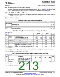
Table 5-80. McSPI Timing Conditions—Slave Mode
TIMING CONDITION PARAMETER
MIN
MAX UNIT
Input Conditions
tr
Input signal rise time
5
5
ns
ns
tf
Input signal fall time
Output Condition
Cload
Output load capacitance
20
pF
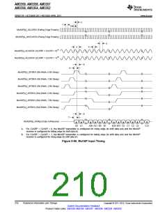
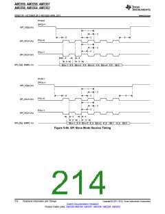
Table 5-81. Timing Requirements for McSPI Input Timings—Slave Mode
(see Figure 5-88)
OPP100
MIN
OPP50
NO.
UNIT
MAX
MIN
MAX
1
2
3
tc(SPICLK)
Cycle time, SPI_CLK
62.5
0.5P(1)
0.5P(1)
124.8
ns
ns
ns
tw(SPICLKL)
tw(SPICLKH)
Typical Pulse duration, SPI_CLK low
Typical Pulse duration, SPI_CLK high
0.5P(1)
0.5P(1)
0.5P(1)
0.5P(1)
0.5P(1)
0.5P(1)
Setup time, SPI_D[x] (SIMO) valid before SPI_CLK
active edge(2)(3)
4
5
tsu(SIMO-SPICLK)
th(SPICLK-SIMO)
tsu(CS-SPICLK)
th(SPICLK-CS)
12.92
12.92
12.92
ns
ns
Hold time, SPI_D[x] (SIMO) valid after SPI_CLK
active edge(2)(3)
12.92
Setup time, SPI_CS valid before SPI_CLK first
edge(2)
Hold time, SPI_CS valid after SPI_CLK last edge(2)
8
9
12.92
12.92
12.92
12.92
ns
ns
(1) P = SPI_CLK period.
(2) This timing applies to all configurations regardless of MCSPIX_CLK polarity and which clock edges are used to drive output data and
capture input data.
(3) Pins SPIx_D0 and SPIx_D1 can function as SIMO or SOMI.
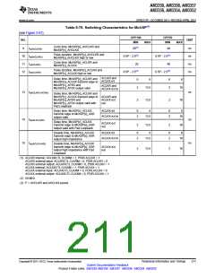
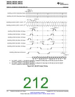
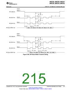
Table 5-82. Switching Characteristics for McSPI Output Timings—Slave Mode
(see Figure 5-89)
OPP100
MIN
OPP50
MIN
NO.
PARAMETER
UNIT
MAX
MAX
Delay time, SPI_CLK active edge to
SPI_D[x] (SOMI) transition(1)(2)
6
7
td(SPICLK-SOMI)
td(CS-SOMI)
-4.00
17.12
-4.00
17.12
ns
ns
Delay time, SPI_CS active edge to
SPI_D[x] (SOMI) transition(1)(2)
17.12
17.12
(1) This timing applies to all configurations regardless of MCSPIX_CLK polarity and which clock edges are used to drive output data and
capture input data.
(2) Pins SPIx_D0 and SPIx_D1 can function as SIMO or SOMI.
Copyright © 2011–2013, Texas Instruments Incorporated
Peripheral Information and Timings
213
Submit Documentation Feedback
Product Folder Links: AM3359 AM3358 AM3357 AM3356 AM3354 AM3352

 TI [ TEXAS INSTRUMENTS ]