AM3359, AM3358, AM3357
AM3356, AM3354, AM3352
www.ti.com
SPRS717F –OCTOBER 2011–REVISED APRIL 2013
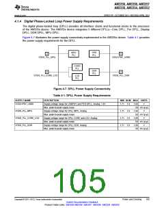
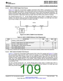
4.2.2.2 OSC0 LVCMOS Digital Clock Source
Figure 4-10 shows the recommended oscillator connections when OSC0 is connected to an LVCMOS
square-wave digital clock source. The LVCMOS clock source is connected to the XTALIN terminal. In this
mode of operation, the XTALOUT terminal should not be used to source any external components. The
printed circuit board design should provide a mechanism to disconnect the XTALOUT terminal from any
external components or signal traces that may couple noise into OSC0 via the XTALOUT terminal.
The XTALIN terminal has a 15 - 40 kΩ internal pull-down resistor which is enabled when OSC0 is
disabled. This internal resistor prevents the XTALIN terminal from floating to an invalid logic level which
may increase leakage current through the oscillator input buffer.
AM335x
XTALIN
VSS_OSC
XTALOUT
VDDS_OSC
LVCMOS
Digital
Clock
Source
Figure 4-10. OSC0 LVCMOS Circuit Schematic
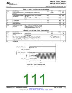
Table 4-4. OSC0 LVCMOS Reference Clock Requirements
NAME
f(XTALIN)
DESCRIPTION
Frequency, LVCMOS reference clock
MIN
TYP
MAX
UNIT
19.2, 24, 25,
or 26
MHz
Frequency, LVCMOS reference clock stability and tolerance(1)
Duty cycle, LVCMOS reference clock period
Jitter peak-to-peak, LVCMOS reference clock period
Time, LVCMOS reference clock rise
-50
45
-1
50
55
1
ppm
%
tdc(XTALIN)
tjpp(XTALIN)
tR(XTALIN)
tF(XTALIN)
%
5
ns
Time, LVCMOS reference clock fall
5
ns
(1) Initial accuracy, temperature drift, and aging effects should be combined when evaluating a reference clock for this requirement.
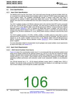
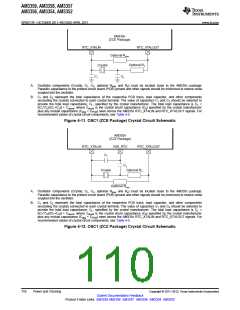
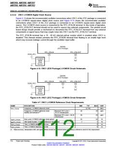
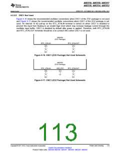
4.2.2.3 OSC1 Internal Oscillator Clock Source
Figure 4-11 shows the recommended crystal circuit for OSC1 of the ZCE package and Figure 4-12 shows
the recommended crystal circuit for OSC1 of the ZCZ package. It is recommended that pre-production
printed circuit board (PCB) designs include the two optional resistors Rbias and Rd in case they are
required for proper oscillator operation when combined with production crystal circuit components. In most
cases, Rbias is not required and Rd is a 0-Ω resistor. These resistors may be removed from production
PCB designs after evaluating oscillator performance with production crystal circuit components installed on
pre-production PCBs.
The RTC_XTALIN terminal has a 10 - 40 kΩ internal pull-up resistor which is enabled when OSC1 is
disabled. This internal resistor prevents the RTC_XTALIN terminal from floating to an invalid logic level
which may increase leakage current through the oscillator input buffer.
Copyright © 2011–2013, Texas Instruments Incorporated
Power and Clocking
109
Submit Documentation Feedback
Product Folder Links: AM3359 AM3358 AM3357 AM3356 AM3354 AM3352

 TI [ TEXAS INSTRUMENTS ]