AM3359, AM3358, AM3357
AM3356, AM3354, AM3352
SPRS717F –OCTOBER 2011–REVISED APRIL 2013
www.ti.com
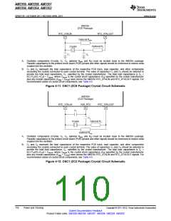
AM335x
(ZCE Package)
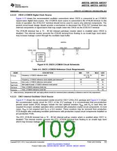
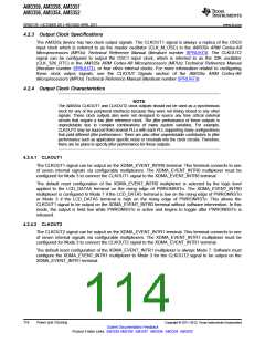
RTC_XTALIN
RTC_XTALOUT
Optional Rbias
Optional Rd
Crystal
C1
C2
A. Oscillator components (Crystal, C1, C2, optional Rbias and Rd) must be located close to the AM335x package.
Parasitic capacitance to the printed circuit board (PCB) ground and other signals should be minimized to reduce noise
coupled into the oscillator.
B. C1 and C2 represent the total capacitance of the respective PCB trace, load capacitor, and other components
(excluding the crystal) connected to each crystal terminal. The value of capacitors C1 and C2 should be selected to
provide the total load capacitance, CL, specified by the crystal manufacturer. The total load capacitance is CL
=
[(C1*C2)/(C1+C2)] + Cshunt, where Cshunt is the crystal shunt capacitance (C0) specified by the crystal manufacturer
plus any mutual capacitance (Cpkg + CPCB) seen across the AM335x RTC_XTALIN and RTC_XTALOUT signals. For
recommended values of crystal circuit components, see Table 4-5.
Figure 4-11. OSC1 (ZCE Package) Crystal Circuit Schematic
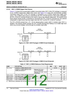
AM335x
(ZCZ Package)
RTC_XTALIN
VSS_RTC
RTC_XTALOUT
C1
C2
Optional Rd
Crystal
Optional Rbias
A. Oscillator components (Crystal, C1, C2, optional Rbias and Rd) must be located close to the AM335x package.
Parasitic capacitance to the printed circuit board (PCB) ground and other signals should be minimized to reduce noise
coupled into the oscillator.
B. C1 and C2 represent the total capacitance of the respective PCB trace, load capacitor, and other components
(excluding the crystal) connected to each crystal terminal. The value of capacitors C1 and C2 should be selected to
provide the total load capacitance, CL, specified by the crystal manufacturer. The total load capacitance is CL
=
[(C1*C2)/(C1+C2)] + Cshunt, where Cshunt is the crystal shunt capacitance (C0) specified by the crystal manufacturer
plus any mutual capacitance (Cpkg + CPCB) seen across the AM335x RTC_XTALIN and RTC_XTALOUT signals. For
recommended values of crystal circuit components, see Table 4-5.
Figure 4-12. OSC1 (ZCZ Package) Crystal Circuit Schematic
110
Power and Clocking
Copyright © 2011–2013, Texas Instruments Incorporated
Submit Documentation Feedback
Product Folder Links: AM3359 AM3358 AM3357 AM3356 AM3354 AM3352

 TI [ TEXAS INSTRUMENTS ]