AM3359, AM3358, AM3357
AM3356, AM3354, AM3352
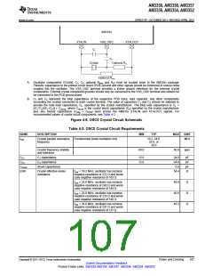
www.ti.com
SPRS717F –OCTOBER 2011–REVISED APRIL 2013
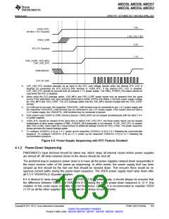
1.8V
VDDS_RTC,
All other 1.8-V Supplies
1.8V/1.5V/1.35V
3.3V
VDDS_DDR
All 3.3-V Supplies
1.1V
VDD_CORE, VDD_MPU
CAP_VDD_RTC
PWRONRSTn
CLK_M_OSC
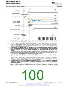
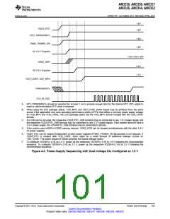
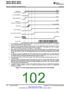
A. CAP_VDD_RTC terminal operates as an input to the RTC core voltage domain when the internal RTC LDO is
disabled by connecting the RTC_KALDO_ENn terminal to VDDS_RTC. If the internal RTC LDO is disabled,
CAP_VDD_RTC should be sourced from an external 1.1-V power supply. The PMIC_POWER_EN output cannot be
used when the RTC is disabled.
B. When using the ZCZ package option, VDD_MPU and VDD_CORE power inputs may be powered from the same
source if the application only uses operating performance points (OPPs) that define a common power supply voltage
for VDD_MPU and VDD_CORE. The ZCE package option has the VDD_MPU domain merged with the VDD_CORE
domain.
C. If a USB port is not used, the respective VDDA1P8V_USB terminal may be connected to any 1.8-V power supply and
the respective VDDA3P3V_USB terminal may be connected to any 3.3-V power supply. If the system does not have a
3.3-V power supply, the VDDA3P3V_USB terminal may be connected to ground.
D. If the system uses mDDR or DDR2 memory devices, VDDS_DDR can be ramped simultaneously with the other 1.8-V
IO power supplies.
E. VDDS_RTC should be ramped at the same time or before CAP_VDD_RTC, but these power inputs can be ramped
independent of other power supplies if PMIC_POWER_EN functionality is not required. If CAP_VDD_RTC is ramped
after VDD_CORE, there might be a small amount of additional leakage current on VDD_CORE. The power sequence
shown provides the lowest leakage option.
F. To configure VDDSHVx [1-6] as 1.8 V, power up the respective VDDSHVx [1-6] to 1.8 V following the recommended
sequence. To configure VDDSHVx [1-6] as 3.3 V, power up the respective VDDSHVx [1-6] to 3.3 V following the
recommended sequence.
Figure 4-5. Power-Supply Sequencing with RTC Feature Disabled
4.1.2 Power-Down Sequencing
PWRONRSTn input terminal should be taken low, which stops all internal clocks before power supplies
are turned off. All other external clocks to the device should be shut off.
The preferred way to sequence power down is to have all the power supplies ramped down sequentially in
the exact reverse order of the power-up sequencing. In other words, the power supply that has been
ramped up first should be the last one that should be ramped down. This ensures there would be no
spurious current paths during the power-down sequence. The VDDS power supply must ramp down after
all 3.3-V VDDSHVx [1-6] power supplies.
If it is desired to ramp down VDDS and VDDSHVx [1-6] simultaneously, it should always be ensured that
the difference between VDDS and VDDSHVx [1-6] during the entire power-down sequence is <2 V. Any
violation of this could cause reliability risks for the device. Further, it is recommended to maintain VDDS
≥1.5V as all the other supplies fully ramp down to minimize in-rush currents.
Copyright © 2011–2013, Texas Instruments Incorporated
Power and Clocking
103
Submit Documentation Feedback
Product Folder Links: AM3359 AM3358 AM3357 AM3356 AM3354 AM3352

 TI [ TEXAS INSTRUMENTS ]